What Is TSV (Through-Silicon Via)? How It Powers HBM, AI Chips, and Advanced Packaging


Hello, this is MasterMind.
As artificial intelligence drives a new wave of semiconductor investment, much of the attention naturally goes to faster GPUs, smaller process nodes, and more powerful AI accelerators.
But there is another question investors should be asking
What happens when processors become faster than the system's ability to feed them data?
This is one of the fundamental challenges facing modern AI computing.
An AI accelerator can perform enormous numbers of calculations, but those computing resources cannot be fully utilized if data cannot move between memory and processors quickly enough.
That is why technologies such as HBM (High Bandwidth Memory), advanced packaging, chiplets, and TSV (Through-Silicon Via) have become increasingly important.
TSV is particularly important because it enables electrical connections to travel vertically through silicon, allowing multiple semiconductor dies to be stacked and interconnected.
Rather than viewing TSV as an obscure manufacturing process, investors can think of it as part of the infrastructure that allows modern AI computing systems to move enormous amounts of data efficiently.
Key takeaway
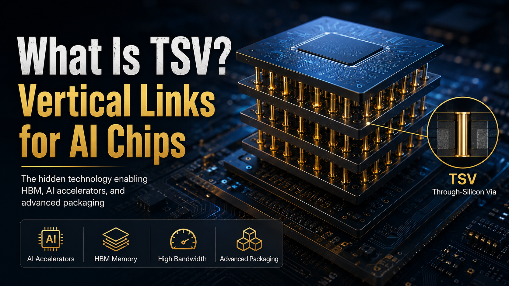
TSV is a semiconductor interconnect technology that creates vertical electrical pathways through silicon. It plays a critical role in stacked-memory architectures such as HBM and is part of the broader shift toward advanced 3D semiconductor packaging.
What Is TSV (Through-Silicon Via)?
TSV stands for Through-Silicon Via.
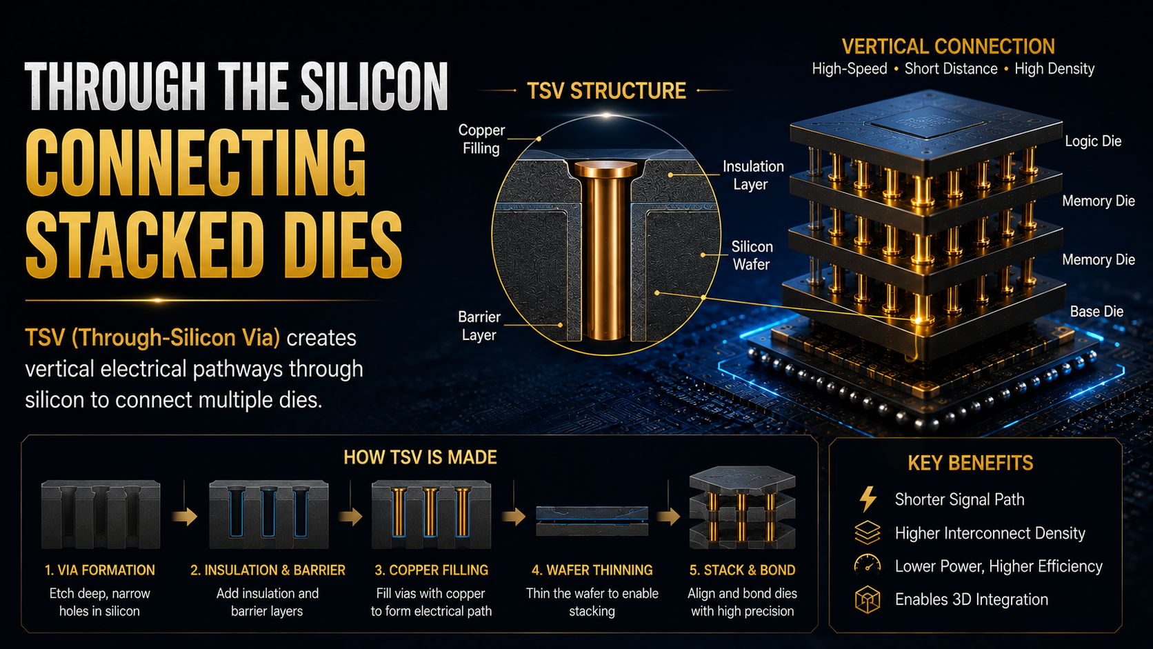
A TSV is essentially a microscopic vertical electrical connection formed through a silicon wafer or semiconductor die.
Engineers create tiny openings through the silicon and fill or line them with conductive materials, commonly including copper, to establish electrical pathways between vertically stacked semiconductor layers.
The easiest way to understand TSV is to think about transportation inside a building.
Traditional chip interconnections can resemble roads that run around the outside of buildings.
TSVs are more like high-speed elevators running directly through the building.
Instead of forcing electrical signals to travel relatively long paths around the edges of a chip, vertical interconnects can provide shorter paths between stacked dies.
This becomes especially valuable when semiconductor manufacturers want to place multiple chips on top of one another.
Traditional Interconnects vs. TSV
| Feature | Traditional Wire-Bond-Based Packaging | TSV |
| Connection structure | Primarily edge/external connections | Vertical connections through silicon |
| Signal distance | Can be relatively longer | Short vertical pathways possible |
| Interconnect density | More structurally constrained | High-density connections possible |
| Packaging direction | Primarily planar | Supports vertical stacking |
| Space efficiency | Requires more lateral space | Improves vertical integration |
| Major applications | Conventional semiconductor packages | HBM and advanced 3D integration |
The real value of TSV is therefore not simply that chips can be stacked.
It is that stacked semiconductor dies can communicate through dense, short electrical pathways.
How Does TSV Technology Work?
The concept sounds straightforward, but manufacturing TSVs is technically demanding.
Several semiconductor processes must work together with extremely high precision.
1. Creating the Via
The process begins by creating extremely small and deep holes in silicon.
Advanced etching processes are typically required to achieve the necessary dimensions and aspect ratios.
The geometry must be carefully controlled because defects can affect electrical performance and manufacturing yield.
2. Adding Insulation and Conductive Layers
The via must be electrically isolated from the surrounding silicon where necessary.
Manufacturers therefore form insulating and barrier structures before creating the final conductive pathway.
3. Filling the Via
Conductive material is deposited into the opening to create the electrical connection.
Copper is commonly associated with TSV structures because of its electrical conductivity and compatibility with semiconductor manufacturing.
4. Thinning the Wafer
Vertical stacking requires semiconductor dies to become extremely thin.
Wafer thinning reduces package thickness and helps expose or integrate the TSV structures required for stacking.
5. Stacking and Bonding the Dies
The dies must then be aligned and bonded with extremely high precision.
Even tiny alignment errors can affect yield and performance.
This is why TSV should not be viewed as a single manufacturing step.
It sits inside a broader ecosystem involving etching, deposition, metallization, wafer thinning, bonding, inspection, and packaging technologies.
Why TSV Matters for HBM
For investors following the AI semiconductor market, the most important application of TSV is High Bandwidth Memory.
HBM is designed to move large quantities of data at very high bandwidth while maintaining a compact physical footprint.
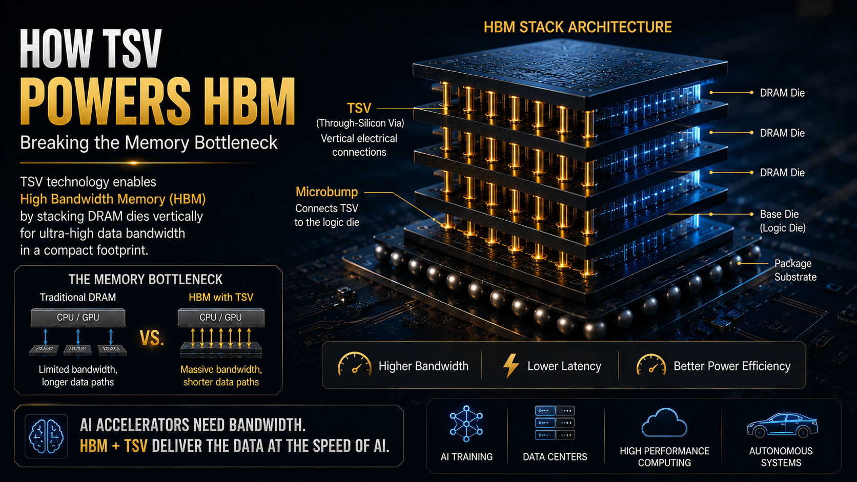
Instead of arranging all memory dies horizontally, HBM stacks multiple DRAM dies vertically.
TSVs provide vertical electrical pathways through the stack.
Conceptually, the architecture looks like this
AI Accelerator / GPU
        │
High-Speed Interface
        │
       HBM
 ┌─────────────┐
 │  DRAM Die   │
 │      │      │
 │     TSV     │
 │      │      │
 │  DRAM Die   │
 │      │      │
 │     TSV     │
 │      │      │
 │  DRAM Die   │
 └─────────────┘
Why does this matter?
Because modern AI accelerators consume data at extraordinary rates.
If the processor can perform calculations faster than memory can supply data, the expensive compute hardware can spend part of its time waiting.
This is part of what is commonly described as the memory wall or memory bottleneck.
HBM helps address this challenge by providing very wide memory interfaces and high bandwidth.
TSV is one of the technologies that makes vertically stacked HBM architectures possible.
AI Computing Is Becoming a Data-Movement Problem
For decades, semiconductor performance was closely associated with transistor scaling.
Smaller transistors allowed chipmakers to place more computing resources into a given area while improving performance and efficiency.
That strategy remains important.
But leading-edge semiconductor manufacturing has become increasingly complex and capital-intensive.
At the same time, AI workloads have introduced another challenge: moving enormous amounts of data between compute, memory, and other components.
This is changing how the industry thinks about semiconductor performance.
The semiconductor race is no longer only about building smaller transistors. It is increasingly about connecting compute, memory, and specialized silicon efficiently enough to make the entire system perform as one.
That shift is driving investment into several interconnected technologies
- HBM
- Advanced packaging
- Chiplets
- Silicon interposers
- TSV
- Die-to-die interconnects
- Advanced bonding technologies
For investors, this represents an important expansion of the semiconductor value chain.
The Shift From Scaling to Advanced Packaging
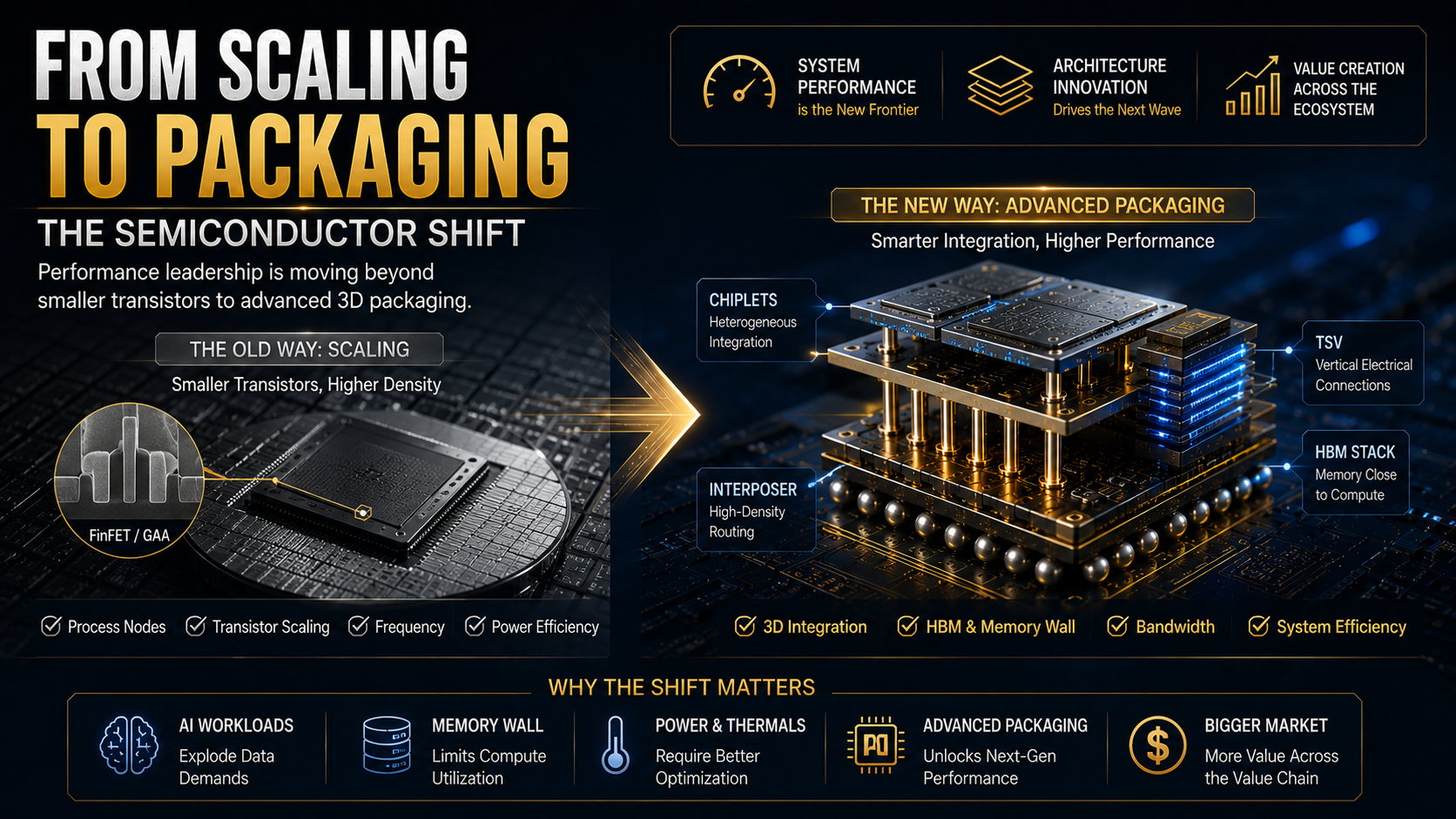
Advanced packaging does not mean semiconductor scaling is becoming irrelevant.
Instead, packaging is becoming another major performance lever alongside transistor improvements.
Historically, much of the industry's competitive advantage was concentrated in front-end manufacturing.
Companies competed heavily around lithography, transistor architecture, and process nodes.
In the AI era, system-level performance increasingly depends on what happens after individual dies have been manufactured.
Different components must be connected efficiently.
Memory must remain physically close to compute.
Power delivery and thermal management must improve.
Communication between dies must become faster.
This makes advanced packaging increasingly strategic.
TSV is one piece of this larger transition.
Benefits of TSV Technology
Higher Interconnect Density
Vertical connections can allow a large number of electrical pathways to exist between stacked semiconductor dies.
That helps support architectures requiring wide data interfaces.
Shorter Signal Paths
Reducing the physical distance between connected dies can improve signal efficiency and help reduce latency.
Better Energy Efficiency
Moving data consumes energy.
Shorter and more efficient interconnect structures can reduce the energy required for data movement compared with less optimized architectures.
This matters increasingly as power consumption becomes one of the largest constraints on AI infrastructure.
Greater Packaging Density
Vertical stacking allows semiconductor designers to increase functional density without relying entirely on horizontal expansion.
This is particularly useful when package area and interconnect length become limiting factors.
TSV Has Important Challenges
Investors should not assume that technological importance automatically means easy economics.
TSV manufacturing introduces significant complexity.
Manufacturing Difficulty
Creating deep, narrow structures through silicon while maintaining consistent electrical characteristics is technically challenging.
Each additional process can increase manufacturing complexity and cost.
Yield
Yield becomes especially important when expensive semiconductor dies are stacked together.
A defect introduced late in the manufacturing process can reduce the economic value of other components already incorporated into the package.
For this reason, manufacturing yield can be as important as technological capability.
Thermal Management
Vertical integration improves density but can complicate heat dissipation.
This becomes particularly important in AI computing systems where high-performance processors already consume substantial amounts of power.
Advanced packaging and cooling therefore increasingly need to be considered together.
Cost
TSV-related manufacturing requires specialized processes and equipment.
Higher performance can justify higher costs in premium AI applications, but economics remain an important factor when technologies move into broader markets.
How TSV Is Changing the Semiconductor Value Chain
TSV itself does not determine stock prices.
The more relevant question for investors is how growing demand for HBM and advanced packaging changes where semiconductor capital expenditures flow.
| Industry Segment | Potential Structural Impact |
| Memory | Greater strategic importance of HBM and high-performance DRAM |
| AI accelerators | Memory bandwidth becomes increasingly important to system performance |
| Semiconductor equipment | Demand for specialized etch, deposition, thinning, bonding and inspection processes |
| Materials | Higher requirements for advanced interconnect and packaging materials |
| Foundries | Packaging capabilities become more strategically important alongside leading-edge fabrication |
| OSAT providers | Advanced assembly and testing capabilities become more valuable |
| Data centers | Compute, memory, networking, power and cooling increasingly optimized as one system |
The important investment insight is the direction of capital.
Money tends to move toward bottlenecks.
If AI accelerator supply expands but HBM capacity becomes constrained, capital moves toward memory.
If HBM production expands but advanced packaging capacity becomes the limiting factor, investment moves toward packaging.
If packaging becomes more sophisticated, demand can migrate toward bonding, inspection, materials, and specialized equipment.
Understanding the bottleneck can therefore be more valuable than simply identifying the fastest-growing end market.
TSV vs. Interposers vs. Hybrid Bonding
These technologies are sometimes discussed as though they are direct substitutes, but they serve different functions within advanced semiconductor packaging.
| Technology | Primary Function |
| TSV | Provides vertical electrical connections through silicon |
| Silicon interposer | Provides high-density connectivity between multiple dies |
| Hybrid bonding | Enables extremely fine-pitch direct connections between dies or wafers |
They can also complement one another within broader packaging architectures.
That distinction matters for long-term investors.
Semiconductor technology rarely develops as a simple winner-takes-all contest between individual manufacturing techniques.
Different architectures can use different combinations depending on performance, cost, thermal requirements, and manufacturing yield.
The more durable investment question is therefore not
"Which packaging technology wins?"
It is
"Which companies remain strategically relevant as packaging architectures evolve?"
What Should Investors Watch?
The first factor is actual HBM demand.
AI infrastructure spending, accelerator shipments, and the memory content required per system can influence demand for advanced memory technologies.
But investors should distinguish between industry growth and expectations already embedded in asset prices.
A rapidly growing industry can still disappoint investors if the market expected even faster growth.
The second factor is advanced packaging capacity.
Manufacturing bottlenecks can migrate through the supply chain. Investors should therefore watch not only semiconductor wafer capacity but also the ability to package complex products at scale.
Third is yield.
Having advanced technology is not enough. A company must manufacture it reliably and economically.
Yield affects cost, margins, production capacity, and ultimately cash generation.
Finally, investors should watch the evolution beyond any single technology.
TSV exists alongside micro-bumps, interposers, chiplets, and increasingly sophisticated bonding techniques.
The broader trend toward higher-density heterogeneous integration is more important than any single acronym.
What Do Long-Term Capital Allocators See in This Trend?
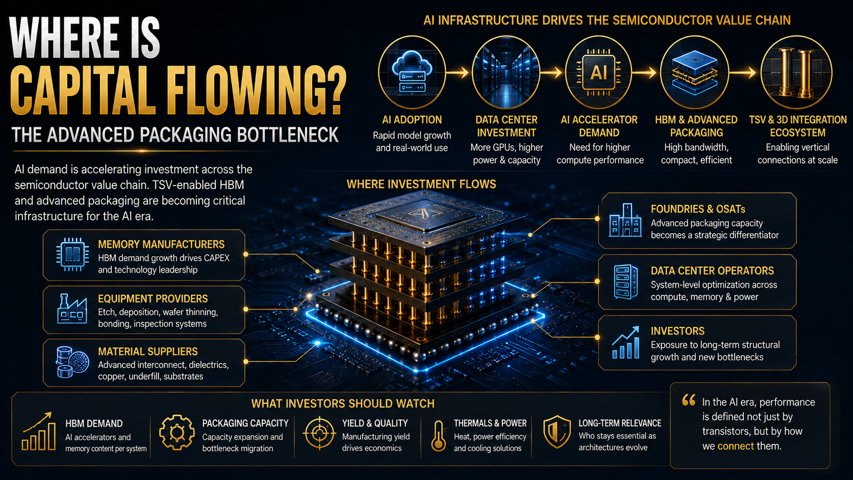
Long-term investors often focus less on the most visible product and more on the infrastructure required to make an entire technology cycle possible.
Follow the Capital
A simplified AI semiconductor capital flow might look like this
AI Adoption
     ↓
Data Center Investment
     ↓
AI Accelerator Demand
     ↓
High-Performance Memory Demand
     ↓
HBM and Advanced Packaging
     ↓
TSV / Bonding / Etch / Inspection / Materials
The important question is where persistent bottlenecks develop.
If a technology becomes essential to removing those bottlenecks, additional capital is likely to be directed toward expanding that capacity.
Follow the Cash Flow
Technological importance and investment quality are not the same thing.
A company can operate in a rapidly expanding market while generating poor returns if capital expenditures rise faster than cash generation or competition destroys margins.
Investors should therefore look beyond revenue growth.
Operating margins, free cash flow, capital intensity, customer concentration, pricing power, and return on invested capital can be equally important.
Look for Survivability
Today's packaging architecture will not necessarily remain unchanged.
Hybrid bonding, new interconnect structures, chiplet architectures, and other technologies will continue to evolve.
A durable company may therefore be one whose expertise can remain relevant across multiple generations of packaging technology rather than one dependent on a single process.
Think Beyond the AI Hype Cycle
There is a popular analogy from the gold rush: instead of trying to identify who would find gold, some investors preferred the businesses supplying essential tools.
A similar framework can be useful in AI infrastructure.
Rather than trying to predict exactly which AI processor will dominate years from now, investors can examine the technologies, equipment, materials, and manufacturing capacity that multiple competing platforms require.
But one qualification is critical
Being essential to the semiconductor industry does not automatically make a company an attractive investment.
Valuation still matters.
Competition still matters.
Capital intensity still matters.
And expectations matter.
A useful question for investors is
Am I investing in a company simply because it is associated with AI and HBM, or does it genuinely solve a persistent semiconductor bottleneck while generating durable cash flow?
Investing is not about predicting every technological shift correctly.
It is about owning assets capable of surviving when those predictions are wrong.
Conclusion
TSV, or Through-Silicon Via, is a technology that creates vertical electrical connections through silicon, allowing semiconductor dies to communicate efficiently in vertically integrated architectures.
Its most visible role today is in high-performance memory such as HBM, where stacked DRAM dies help deliver the enormous memory bandwidth required by modern AI accelerators.
But the larger investment story goes beyond TSV itself.
The semiconductor industry's competitive landscape is expanding from a race centered primarily on transistor scaling toward a much broader contest involving memory bandwidth, chiplets, advanced packaging, interconnects, power efficiency, and system-level integration.
That transition can redirect capital across the semiconductor supply chain.
Memory manufacturers, foundries, packaging providers, equipment companies, materials suppliers, and data-center infrastructure providers can all be affected as the industry's bottlenecks change.
For long-term investors, the goal should not be to chase every new semiconductor acronym.
The more useful approach is to understand what problem the technology solves, where the bottleneck is moving, where capital expenditures are flowing, and which companies can convert that investment cycle into sustainable cash flow.
The key idea to remember is simple
The AI semiconductor race is not only about computing faster. It is also about moving more data over shorter distances with greater efficiency. TSV is one of the technologies helping make that possible.
This was MasterMind.
'[Global] Success Blueprints' 카테고리의 다른 글