What Is 2.5D Packaging? How It Connects AI GPUs, HBM, and Chiplets


Hello, this is MasterMind.
For decades, the semiconductor industry improved performance primarily by shrinking transistors. Smaller process nodes allowed chipmakers to pack more transistors into the same area while improving computing performance and power efficiency.
That strategy still matters, but it is no longer the entire story.
The rise of artificial intelligence has created another challenge: moving enormous amounts of data between processors and memory quickly enough to keep expensive AI accelerators fully utilized.
A powerful GPU cannot deliver its theoretical performance if it spends too much time waiting for data from memory.
This is why terms such as 2.5D packaging, HBM, chiplets, silicon interposers, and advanced packaging have become increasingly important to investors following the AI semiconductor industry.
The semiconductor race is expanding from simply building faster chips to connecting multiple high-performance chips into a faster system.
And 2.5D packaging sits at the center of that transition.
Key Takeaway
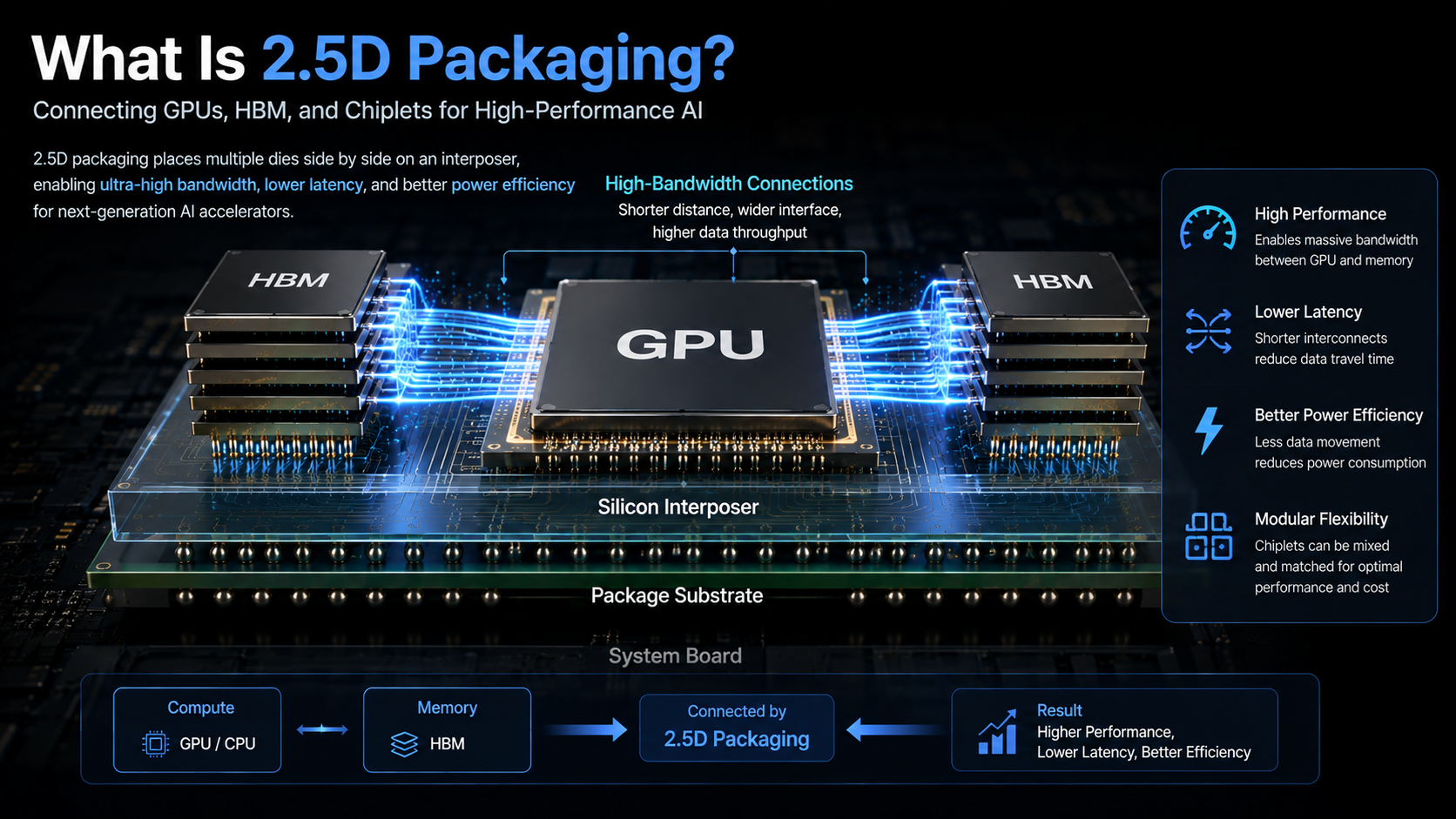
2.5D packaging is an advanced semiconductor packaging architecture that places GPUs, CPUs, HBM, and other chiplets close together on a high-density interconnect layer such as a silicon interposer. As transistor scaling becomes more difficult and AI workloads demand massive memory bandwidth, advanced packaging is becoming an increasingly important part of overall system performance.
What Is 2.5D Packaging?
2.5D packaging is a semiconductor packaging architecture in which multiple dies are placed side by side on an interposer, allowing them to communicate through dense, short electrical connections.
A simplified AI accelerator architecture might look like this
GPU / Compute Dies
↓
High-Density Connections
↓
Interposer
↔
HBM Stacks
↓
Package Substrate
↓
System Board
Think of the GPU and memory as buildings in a large city.
Traditional packaging may require data to travel through relatively longer roads between those buildings.
With 2.5D packaging, the buildings are placed much closer together and connected by a dense network of short, high-capacity highways.
The result can be significantly higher bandwidth and more efficient communication between components.
Why Is It Called 2.5D Packaging?
The name describes where the architecture sits between traditional planar packaging and fully stacked 3D integration.
Traditional packaging generally connects chips through a package substrate or board.
In 3D packaging, semiconductor dies can be stacked vertically.
2.5D packaging takes a different approach.
Multiple dies remain largely side by side, but they sit on a high-density interconnect layer that provides far more sophisticated communication than conventional package-level connections.
| Architecture | Traditional Packaging | 2.5D Packaging | 3D Packaging |
| Basic structure | Chip connected through substrate | Multiple dies connected through interposer | Dies vertically stacked |
| Interconnect density | Lower | High | Very high |
| Chip-to-chip distance | Relatively longer | Short | Potentially extremely short |
| Integration | Lower | High | Very high |
| Thermal complexity | Lower | Higher | Potentially much higher |
| Common use cases | General semiconductors | AI accelerators, GPUs, HBM, HPC | Highly integrated computing systems |
Importantly, 3D packaging should not automatically be viewed as the replacement for 2.5D packaging.
Different products have different requirements for cost, thermal management, yield, performance, and manufacturing complexity.
The semiconductor industry is therefore likely to use multiple advanced packaging architectures rather than converge on a single universal solution.
What Is an Interposer?
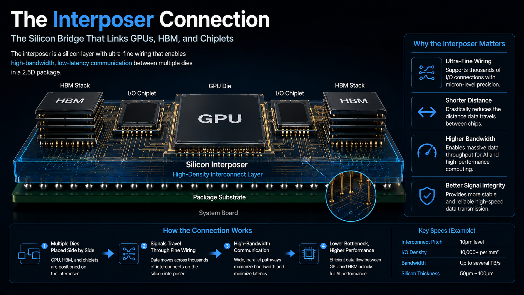
The interposer is one of the most important components of many 2.5D packaging architectures.
It acts as a high-density communication layer between different semiconductor dies.
Silicon interposers can support much finer wiring than conventional package substrates, allowing a large number of signals to travel between components over short distances.
This becomes particularly important for AI accelerators.
Modern AI workloads require enormous quantities of data to move continuously between the processor and memory.
The challenge is not simply computing speed.
It is bandwidth.
Imagine a highway.
Making each individual vehicle faster helps, but once millions of vehicles need to travel simultaneously, the width of the highway becomes equally important.
AI computing faces a similar problem.
As computational throughput rises, processors need increasingly large amounts of data.
Advanced packaging helps create wider communication pathways between compute and memory.
Why 2.5D Packaging Matters as Moore's Law Slows
For decades, semiconductor economics were heavily driven by transistor scaling.
Moving to smaller process nodes allowed chipmakers to increase transistor density and improve performance.
But advanced process nodes have become increasingly difficult and expensive to develop and manufacture.
Large monolithic chips also create additional challenges.
The larger the die, the more difficult yield economics can become because a manufacturing defect may affect a larger and more expensive piece of silicon.
This is where advanced packaging becomes strategically important.
Instead of relying exclusively on transistor scaling, semiconductor companies can improve system performance through a combination of
Advanced Process Nodes + Chiplets + HBM + Advanced Packaging
This does not mean advanced packaging replaces transistor scaling.
The two technologies increasingly complement each other.
The important structural shift is that semiconductor performance is no longer determined only by what happens inside one chip.
It increasingly depends on how effectively multiple chips work together as a system.
How Does 2.5D Packaging Work?
The architecture can be understood through three basic steps.
1. Divide Functions Across Multiple Dies
Instead of placing every function on one enormous monolithic die, designers can distribute different functions across multiple dies or chiplets.
These might include
- compute dies
- I/O dies
- memory interfaces
- networking functions
- specialized accelerators
Different components can potentially be manufactured using process technologies optimized for their specific functions.
2. Place the Dies on an Interposer
The dies are positioned close together on an interposer or another high-density interconnect structure.
Fine wiring allows the chips to communicate through many parallel electrical pathways.
3. Reduce the Data-Movement Bottleneck
Shorter distances and wider interfaces allow large amounts of data to move between chips more efficiently.
This is particularly valuable when connecting processors to HBM.
The result is not simply a faster chip.
It is a more efficient computing system.
Why Are 2.5D Packaging and HBM Closely Connected?
Investors researching advanced packaging will frequently encounter another term: HBM, or High Bandwidth Memory.
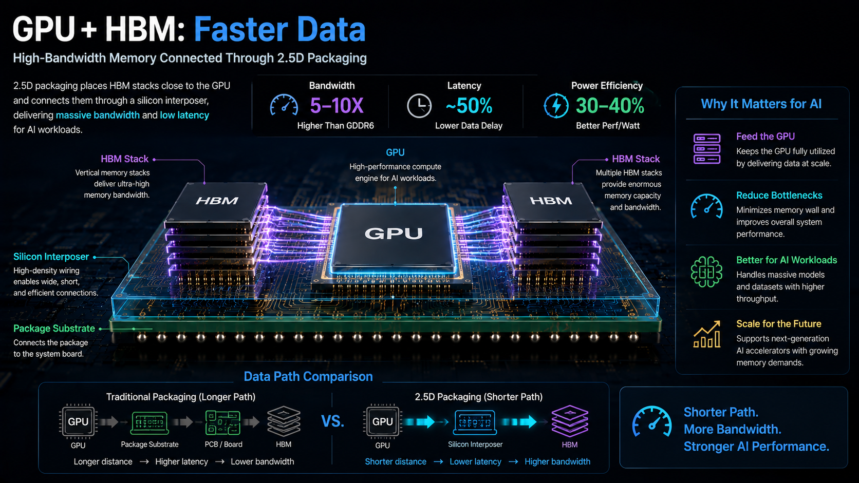
HBM vertically stacks multiple DRAM dies to provide very high memory bandwidth.
But fast memory alone is not enough.
The data stored inside HBM still needs to reach the GPU efficiently.
That creates a critical connection
HBM → Interposer → GPU
By placing HBM stacks close to a GPU and connecting them through high-density interconnects, an AI accelerator can move enormous amounts of data between memory and compute.
This is one reason investors should avoid analyzing the AI semiconductor industry as simply a GPU market.
A more complete supply chain looks like this
AI Accelerators → HBM → Interposers → Advanced Packaging → Package Substrates → Assembly and Test
Every powerful AI accelerator depends on a much larger manufacturing ecosystem.
Why Chiplets Make Advanced Packaging Even More Important
Another structural change supporting advanced packaging is the rise of chiplet architectures.
Historically, semiconductor companies often tried to integrate as many functions as possible onto one large monolithic die.
But larger dies can become increasingly expensive and difficult to manufacture efficiently.
Chiplets offer another approach.
Instead of building one enormous chip, manufacturers can create smaller functional dies and integrate them into a larger system.
A computing package might combine
- CPU or GPU compute chiplets
- I/O chiplets
- networking components
- specialized accelerators
- HBM
Once semiconductor architecture moves in this direction, the ability to connect chips efficiently becomes strategically important.
Packaging therefore begins to move beyond its traditional role as the final manufacturing step.
It becomes part of system architecture itself.
Why Is 2.5D Packaging Difficult to Manufacture?
At first glance, placing several chips on an interposer may sound relatively straightforward.
In practice, advanced packaging introduces significant manufacturing challenges.
Expensive compute dies and HBM stacks must be positioned precisely.
Large numbers of microscopic connections must function reliably.
As package sizes increase, manufacturers must also manage challenges involving
- thermal expansion
- package warpage
- heat dissipation
- interconnect reliability
- assembly precision
- manufacturing yield
Yield is especially important.
A package may contain several expensive semiconductor components. Even if those components were individually functional before assembly, problems during the packaging process can reduce the economics of the final product.
For investors, advanced packaging capacity therefore should not be measured only by theoretical production volume.
A more useful framework is
Capacity + Yield + Thermal Management + Testing + Manufacturing Precision
The ability to manufacture advanced packages reliably at scale can become a competitive advantage.
How 2.5D Packaging Is Reshaping the Semiconductor Supply Chain
The growth of advanced packaging potentially redistributes economic value across a broader semiconductor ecosystem.
| Industry | Potential Impact |
| Foundries and advanced packaging | Greater strategic value for high-volume advanced packaging capacity |
| HBM manufacturers | Growing importance as AI accelerators demand higher memory bandwidth |
| Interposer technologies | Critical connection layer between compute, memory, and chiplets |
| Package substrates | More complex packages require increasingly sophisticated substrates |
| Semiconductor equipment | Greater demand for advanced bonding, packaging, and inspection technologies |
| Materials | Higher requirements for interconnect, thermal, and packaging materials |
| AI infrastructure | Packaging capacity can influence the availability of AI accelerators |
This leads to an important investing principle.
The most important part of a growing industry is not always the product receiving the most attention. Sometimes it is the bottleneck preventing the industry from producing more of that product.
Capital often begins moving toward those bottlenecks when demand grows faster than supply.
What Does 2.5D Packaging Mean for Investors?
Advanced packaging is primarily a semiconductor technology trend, so its most direct financial impact appears across the semiconductor and AI infrastructure industries.
But U.S. investors should think about it within a broader capital-spending cycle.
Semiconductor Stocks
Increasing demand for AI accelerators can create opportunities across HBM, advanced packaging, substrates, semiconductor equipment, testing, and specialized materials.
However, industry growth does not guarantee stock returns.
Revenue growth, margins, competitive positioning, capital intensity, valuation, and future supply all matter.
Big Tech Capital Expenditures
Much of the demand for AI hardware ultimately originates from spending by hyperscalers, cloud providers, and data-center operators.
If AI capital expenditures continue expanding, demand can move upstream through the semiconductor supply chain.
If those capital expenditures slow, the effects can also travel backward through the same chain.
For investors, semiconductor demand therefore needs to be connected to end-market cash flows and capital spending.
Bonds and Interest Rates
2.5D packaging itself does not determine Treasury yields.
But the larger AI infrastructure boom requires enormous amounts of capital for semiconductor fabrication, data centers, networking equipment, cooling systems, and power infrastructure.
Financing conditions and interest rates can therefore affect the pace and economics of the broader investment cycle.
The U.S. Dollar
The semiconductor industry operates through a global supply chain, while much of its trade and financing is linked to the U.S. dollar.
A strong dollar and tight global financial conditions can affect capital spending and financing costs across parts of the supply chain.
Gold and Bitcoin
There is no strong direct economic relationship between 2.5D packaging and gold or Bitcoin.
Those assets tend to respond more directly to variables such as real interest rates, liquidity, the dollar, inflation expectations, and risk sentiment.
Investors should therefore avoid assuming that every asset connected loosely to the technology cycle will move in the same direction.
Five Things Investors Should Watch
1. Where Is the Real Bottleneck?
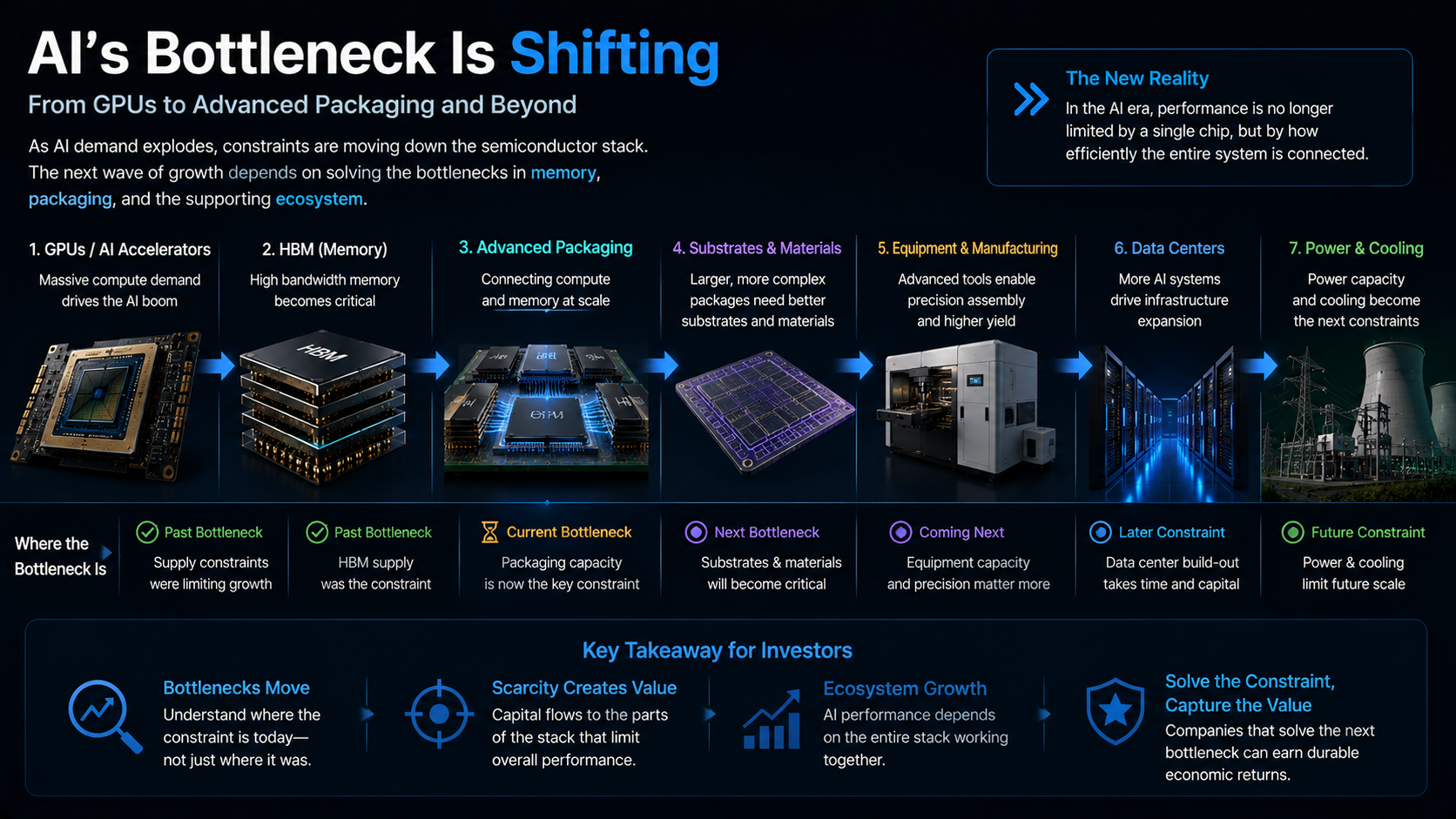
The bottleneck in AI infrastructure can move.
At one point it may be GPUs.
At another, it may be HBM, advanced packaging, substrates, networking equipment, power availability, or data-center capacity.
Rather than simply asking which market is growing fastest, investors should ask
Where is demand currently growing faster than supply?
2. Capacity Is Not the Same as Usable Capacity
A company may announce substantial manufacturing expansion.
But advanced packaging requires reliable high-volume production.
Yield, utilization, customer qualification, and production efficiency can matter as much as headline capacity.
3. What Happens After the Shortage?
Today's bottleneck can become tomorrow's oversupplied market.
High margins during periods of limited supply can attract significant new investment.
Eventually, new capacity may reduce scarcity and change industry economics.
Investors therefore need to think one step beyond the current shortage.
4. Watch Alternative Packaging Technologies
Silicon interposers are important, but semiconductor packaging continues to evolve.
Alternative interconnect structures, organic materials, bridge technologies, and glass-based substrates may play larger roles depending on cost and performance requirements.
The durable investment question is therefore not
Will one specific packaging architecture dominate forever?
A better question is
Which companies can continue solving the industry's interconnect problem as technology changes?
5. Follow AI Capital Expenditures
Advanced packaging demand ultimately depends on real semiconductor demand.
Investors should monitor areas such as
- hyperscaler capital expenditures
- AI accelerator deployments
- HBM supply and demand
- data-center construction
- semiconductor equipment spending
- power infrastructure investment
These indicators can help determine whether demand is becoming structural or simply reflecting a temporary investment surge.
What Do Long-Term Investors See in This Trend?
Long-term investors should look beyond the technology itself and follow the movement of capital.
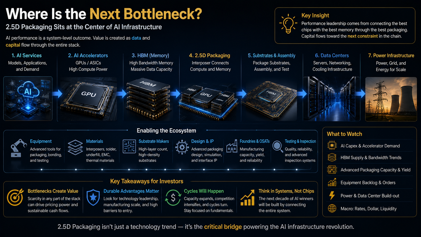
The AI investment chain can be viewed as
AI Services → AI Accelerators → HBM → Advanced Packaging → Equipment and Materials → Data Centers → Power Infrastructure
At the beginning of an investment cycle, market attention may concentrate on GPU designers.
As GPU production expands, demand for HBM rises.
More HBM and compute capacity require more advanced packaging.
More packaging requires additional equipment, substrates, materials, testing, and manufacturing capacity.
Once those AI systems are deployed, capital spending moves further downstream into servers, networking, cooling, data centers, and electricity infrastructure.
The opportunity therefore extends far beyond one semiconductor company.
But capital flows alone do not determine long-term investment returns.
Investors still need to ask whether companies can convert technological importance into sustainable free cash flow.
Can the company maintain high utilization after capacity expands?
Can it protect margins when competitors enter the market?
Does it have a platform that can adapt if today's packaging architecture changes?
Can its balance sheet survive a semiconductor downturn?
These questions matter because technology cycles move quickly.
The strongest long-term assets are not necessarily the companies associated with the most exciting technology.
They are often the businesses capable of surviving multiple generations of technological change.
Two questions are particularly useful
If AI infrastructure spending continues to grow, where will the next supply-chain bottleneck emerge?
And can the companies solving that bottleneck turn scarcity into sustainable cash flow?
That distinction separates following a technology trend from understanding the economics behind it.
Final Thoughts
2.5D packaging is an advanced semiconductor architecture that connects multiple high-performance dies through a dense interconnect layer such as an interposer.
Its importance is growing because AI computing requires more than faster processors.
It requires GPUs, HBM, chiplets, substrates, and interconnect technologies to function together as one high-performance system.
That represents a broader change in the semiconductor industry.
The traditional question was
How much more performance can we extract from a single piece of silicon?
The emerging question is
How efficiently can we connect multiple specialized chips into one computing system?
For investors, understanding 2.5D packaging therefore provides more than knowledge of another semiconductor technology.
It provides a framework for understanding where technological bottlenecks — and potentially capital — may move next across the AI infrastructure supply chain.
The key lesson is simple
As semiconductor competition expands from transistor scaling toward system-level integration, advanced packaging becomes an increasingly important part of the economics of AI computing.
And in investing, predicting every technological winner is less important than identifying businesses capable of generating durable cash flows and surviving as the technology cycle evolves.
This was MasterMind.
'[Global] Success Blueprints' 카테고리의 다른 글