What Is a Glass Substrate? Why It Matters for AI Chip Packaging and Advanced Semiconductors


Hello, this is MasterMind.
For most of semiconductor history, better performance meant one thing: making transistors smaller.
That formula still matters. But the AI era is changing the nature of the semiconductor race.
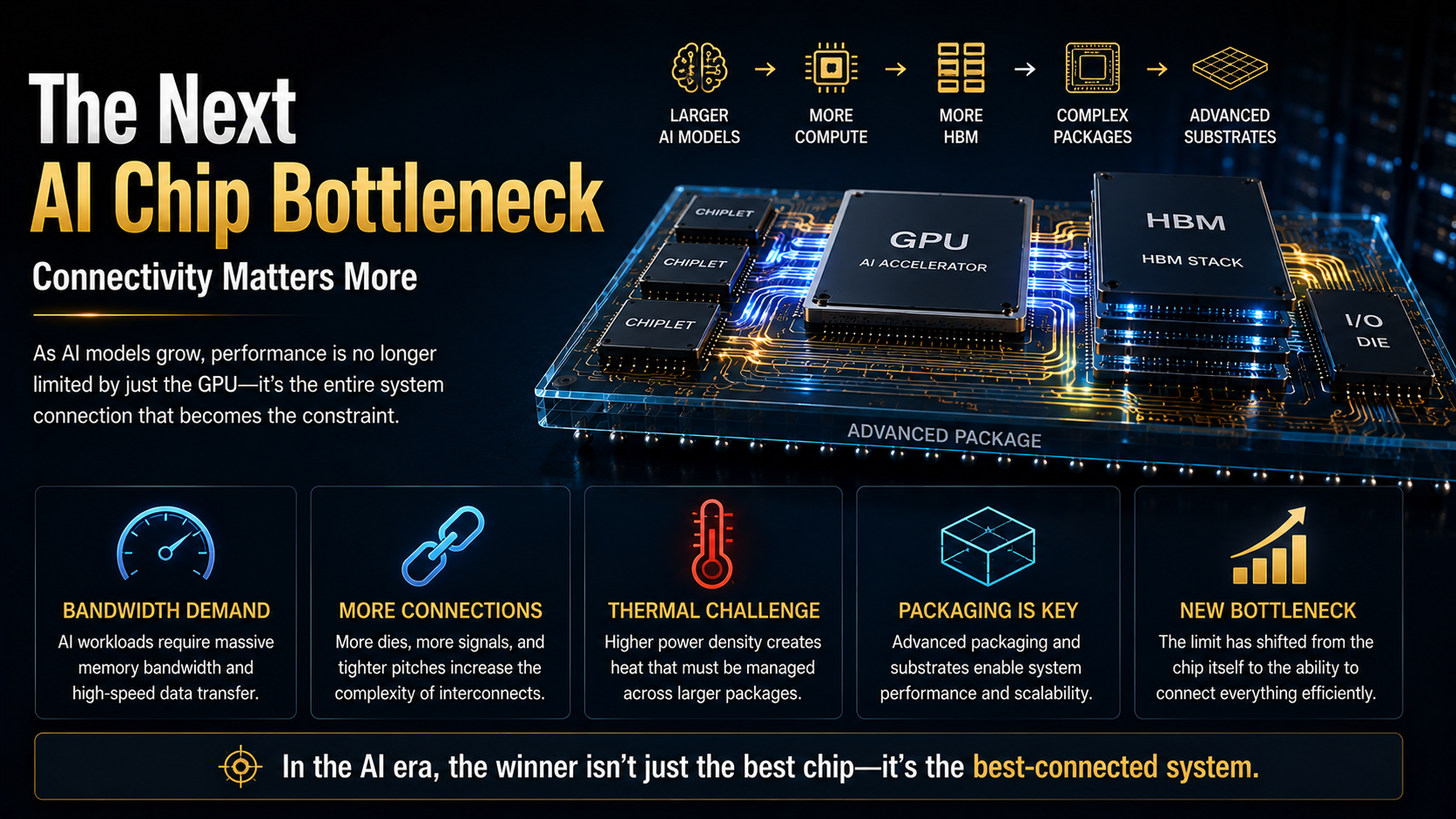
Modern AI accelerators are no longer just individual chips. They are increasingly complex systems that combine GPUs, high-bandwidth memory (HBM), chiplets, I/O components, and high-speed interconnects inside increasingly sophisticated packages.
That creates a new question for the semiconductor industry
What happens when the chips keep getting better, but the package connecting them becomes the bottleneck?
This is where glass substrate technology enters the discussion.
Glass substrates are being explored as a potential next-generation packaging platform because their material properties may help semiconductor manufacturers build larger, denser, and more dimensionally stable packages.
For investors, however, the important story is not simply that "glass is replacing plastic."
The bigger story is that AI performance is increasingly determined by the entire computing system—not just the transistor.
The Bottom Line
Glass substrates could help overcome some of the warpage, dimensional stability, fine-pitch routing, and scaling challenges associated with increasingly large AI semiconductor packages, making them a potentially important part of next-generation advanced packaging.
What Is a Glass Substrate?
A semiconductor package needs an interface between the silicon and the outside system.
The circuits inside an advanced processor are extraordinarily small, while the connections on a motherboard operate at a much larger scale. A package substrate helps bridge that gap while providing electrical connections, power delivery, and mechanical support.
Think of it as a highly sophisticated transportation network.
If the GPU, HBM, and chiplets are buildings in a city, the package substrate is the network of roads that allows information and power to move between them and the outside world.
As AI processors become more complex, those roads need to become
- narrower,
- more numerous,
- more precisely positioned,
- and capable of supporting larger packages.
Today's high-performance semiconductor packages commonly rely on organic substrate technologies.
These technologies are mature and continue to improve. But as package dimensions and interconnect density increase, issues such as warpage, dimensional stability, routing density, signal integrity, and power delivery become increasingly difficult engineering challenges.
A glass substrate uses glass-based material as part of the packaging structure to potentially address some of those constraints.
Why Are Traditional Substrates Facing New Challenges?
The easiest way to understand the glass substrate opportunity is to look at how semiconductor performance scaling is changing.
For decades, the dominant model was
Smaller transistors → more transistors per chip → better performance
That model has not disappeared.
But leading-edge semiconductor manufacturing has become extraordinarily expensive and technically demanding.
As a result, chipmakers are increasingly combining transistor scaling with another strategy
advanced packaging.
Instead of placing every function on one enormous piece of silicon, semiconductor designers can combine multiple specialized dies within a package.
This is the foundation of the chiplet architecture.
An advanced AI package may eventually combine several components, including
- GPUs or AI accelerators,
- HBM stacks,
- CPU components,
- I/O dies,
- specialized chiplets,
- high-speed interconnects,
- and sophisticated power-delivery structures.
The challenge is straightforward.
As more components are integrated, the package becomes larger and more complicated.
And the larger the package becomes, the more difficult it can be to maintain precise alignment and mechanical stability.
Why Warpage Matters
Semiconductor packages experience repeated temperature changes during manufacturing and operation.
Different materials expand and contract at different rates when temperatures change. This behavior is described by the coefficient of thermal expansion, or CTE.
When multiple materials with different characteristics are combined inside a large package, thermal stress can contribute to warpage.
In simple terms, the package can bend.
At smaller dimensions, these effects may be manageable. But as packages become larger and interconnect pitches become finer, even relatively small dimensional changes can become increasingly important.
Warpage can complicate
- alignment,
- bonding,
- electrical connectivity,
- manufacturing yield,
- and long-term reliability.
This is one reason dimensional stability has become an increasingly important consideration in advanced semiconductor packaging.

Why Use Glass?
Glass has several characteristics that make it interesting for advanced packaging.
The opportunity is not that glass is universally superior to organic substrates.
Rather, certain glass properties may become increasingly valuable as AI packages become larger and more complex.
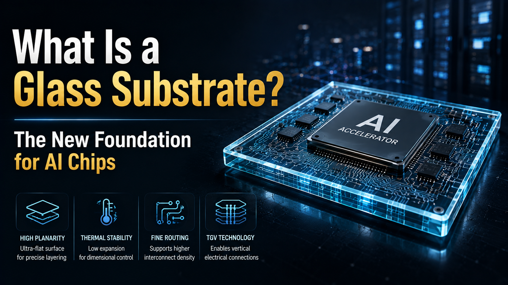
1. High Planarity and Dimensional Stability
Advanced packaging requires extremely precise circuit patterns.
If the underlying substrate changes dimensions during processing, maintaining accurate alignment becomes more difficult.
Glass can offer high planarity and dimensional stability, potentially supporting increasingly precise package structures.
This becomes particularly relevant as package dimensions increase.
A tiny positional error can become much more significant across a large package containing multiple high-value dies.
2. Potential for Finer Routing
AI accelerators move enormous quantities of data between processors and memory.
That means the package itself needs increasingly dense electrical connections.
More routing density can allow more signals to move through a given area.
Glass-based structures may provide additional opportunities for fine-line routing and high-density interconnects, depending on the manufacturing process and package architecture.
3. Potential Advantages for Large Packages
The AI industry is gradually moving away from thinking about processors as isolated chips.
The package is increasingly becoming a computing system.
As more HBM, chiplets, and I/O components are integrated, package dimensions may continue to expand.
That increases the value of materials and manufacturing processes capable of maintaining dimensional stability across larger areas.
4. Through-Glass Vias
Another important technology associated with glass substrates is the Through-Glass Via, or TGV.
A TGV is a small vertical opening formed through glass and filled or lined with conductive material to create an electrical connection through the substrate.
Conceptually, it is similar to a Through-Silicon Via, or TSV, except the vertical connection passes through glass rather than silicon.
TGV structures could enable more flexible vertical signal and power-routing architectures.
The actual performance benefits, however, depend on the complete package design, materials, manufacturing process, and interconnect architecture—not on the via technology alone.

Why Glass Substrates Matter for AI Chips
The AI semiconductor boom is fundamentally about computing capacity.
As AI models become more demanding, the industry needs more compute.
But increasing GPU performance alone does not solve the entire problem.
A processor that cannot receive data quickly enough can spend valuable time waiting for memory.
That is one reason HBM has become so important to AI accelerators.
The broader chain looks something like this
Larger AI models
→ More computing demand
→ More powerful AI accelerators
→ Greater HBM requirements
→ More chiplets and high-speed interconnects
→ Larger and more complex packages
→ Greater demand for advanced packaging
→ More demanding substrate requirements
Glass substrates sit near the end of this chain.
They are not the source of AI compute.
They are infrastructure that could help make increasingly sophisticated AI computing systems physically possible.
The Semiconductor Race Is Moving Beyond the Transistor
This is the larger investment theme.
The semiconductor industry is not abandoning Moore's Law.
Leading-edge transistor technology will remain critically important.
But performance improvements increasingly come from multiple sources.
One is better transistors.
Another is better system integration.
That means the industry is increasingly competing across
process technology + memory + chiplets + interconnects + packaging + power delivery
This changes how investors should think about semiconductor value creation.
A company does not necessarily need to manufacture the fastest GPU to participate in AI infrastructure spending.
Value can also emerge from technologies that remove the bottlenecks surrounding those GPUs.
Markets often follow bottlenecks. Once one constraint is relieved, capital begins searching for the next technology limiting system performance.
Glass Substrates vs. Organic Substrates
The emergence of glass does not mean organic substrates are about to disappear.
Existing substrate technologies have mature manufacturing ecosystems, established supply chains, and significant cost advantages.
They are also continuing to improve.
The relevant question is therefore not
"Is glass technologically better?"
It is
"Can glass provide enough performance and manufacturing advantages to justify the cost and complexity of switching?"
| Category | Organic Substrates | Glass-Based Substrates |
| Industry maturity | Highly established | Earlier development and commercialization stage |
| Manufacturing ecosystem | Mature | Still developing |
| Large-package scaling | Warpage and dimensional control become important | Potential dimensional-stability advantages |
| Planarity | Advanced and improving | Potentially strong material advantage |
| Fine routing | Mature, continuously improving | Potential for additional density |
| Vertical connections | Established via technologies | TGV architectures possible |
| Cost | Benefits from established scale | Potentially higher during early adoption |
| Main challenge | Scaling to increasingly demanding packages | Yield, processing, reliability, and economics |
This distinction is critical for investors.
In semiconductor manufacturing, the technically most impressive solution does not automatically win.
The winner is often the technology that provides the required performance at acceptable cost, yield, reliability, and production scale.
How Glass Substrates Could Affect the Semiconductor Supply Chain
If glass substrates achieve meaningful commercial adoption, the opportunity would extend beyond substrate manufacturers.
A new material often requires new manufacturing processes.
New processes require equipment.
And new equipment creates new supplier ecosystems.
AI Chip Designers
More scalable packaging could provide chip designers with additional flexibility when integrating GPUs, memory, and specialized chiplets into larger systems.
The key question is whether glass can deliver meaningful performance or manufacturing benefits in commercial products.
Substrate Manufacturers
Existing substrate manufacturers may need new production capabilities, equipment, and process expertise.
But building a factory does not guarantee success.
Customer qualification and production yield ultimately matter more than announced capacity.
Materials Suppliers
Potential beneficiaries could extend beyond glass itself.
Advanced packaging requires conductive materials, insulating materials, bonding technologies, and other specialized inputs.
Semiconductor Equipment
Glass processing could create demand for technologies involved in
- precision drilling,
- laser processing,
- TGV formation,
- metallization,
- inspection,
- metrology,
- and advanced patterning.
This is why investors should examine the entire value chain rather than focusing only on companies with "glass substrate" in their corporate presentations.
Following the AI Capital Spending Trail
One of the most useful ways to understand the AI infrastructure cycle is to follow the money.
Early in the AI boom, attention concentrated heavily on GPUs.
Then another bottleneck became obvious
memory bandwidth.
That pushed HBM into the center of the AI semiconductor story.
But GPUs and HBM still need to be integrated into increasingly complex systems.
That elevated advanced packaging.
As packaging becomes larger and denser, attention can move further down the stack toward substrates, interconnect technologies, materials, and manufacturing equipment.
The capital flow can be simplified as
AI data centers
→ GPUs and AI accelerators
→ HBM
→ Advanced packaging
→ Interposers and substrates
→ Glass materials
→ TGV and processing equipment
→ Inspection and metrology
Not every stage will capture the same economics.
And not every technology will become a large market.
But the framework is valuable because it shifts the investor's question from
"What is the next AI stock?"
to
"Where is the next bottleneck, and where will capital have to flow to solve it?"
What Investors Should Watch
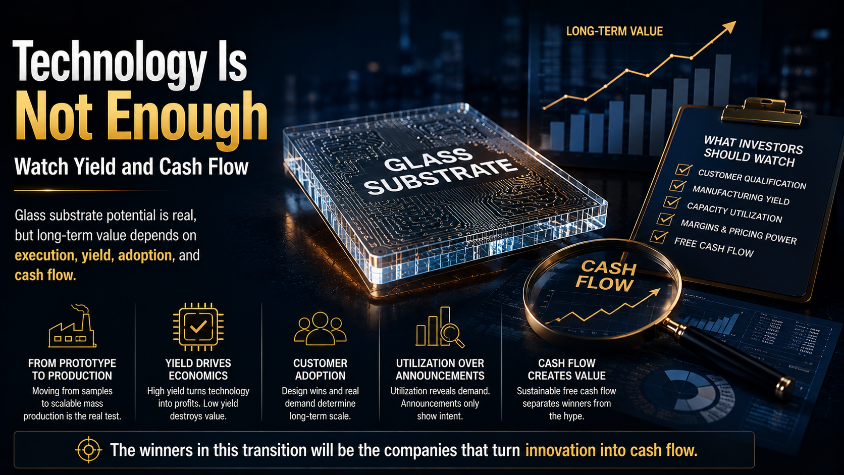
The biggest mistake investors can make with an emerging semiconductor technology is confusing technological progress with commercial success.
New semiconductor technologies typically move through several stages
Development → Prototype → Customer testing → Qualification → Initial production → Yield improvement → High-volume manufacturing
Equity markets can price in enormous future revenue during the first few stages.
Cash flow usually arrives much later.
That gap matters.
1. Development Is Not Mass Production
A company demonstrating a glass substrate is not the same as a company manufacturing millions of economically viable units.
Glass presents its own manufacturing challenges, including handling, cutting, drilling, and defect management.
The critical question is whether the process can achieve acceptable yield at scale.
2. Customer Qualification Matters
The semiconductor industry has demanding qualification standards.
A prototype or sample shipment should not automatically be interpreted as a high-volume commercial contract.
Investors should distinguish among
technical collaboration, sampling, qualification, design wins, purchase commitments, and actual production revenue.
Those milestones are not interchangeable.
3. Yield May Determine the Economics
Yield measures how much of what a factory produces can ultimately be sold as usable product.
A technically impressive process with poor yield can become economically unattractive.
This is particularly important in advanced packaging, where expensive components may be integrated into a single system.
4. Utilization Matters More Than Announced Capacity
Companies often announce new production lines years before demand is fully established.
Capacity tells investors what a company hopes to produce.
Utilization helps reveal whether customers actually want it.
Capex represents expectations. Utilization provides evidence of demand.
5. Follow Free Cash Flow
Emerging semiconductor manufacturing technologies can require substantial capital expenditures.
That creates a crucial distinction between revenue growth and value creation.
Investors should watch
- operating cash flow,
- free cash flow,
- capital expenditures,
- depreciation,
- margins,
- and balance-sheet leverage.
A booming market does not guarantee attractive economics for every supplier.
6. Never Assume the Existing Technology Stops Improving
Glass substrates are not competing against a frozen alternative.
Organic substrates, interposers, packaging architectures, and manufacturing processes will continue to improve.
For glass to gain meaningful adoption, its advantages need to become large enough to justify the switching costs.
The Major Risks
Emerging technologies almost always look easiest before mass production begins.
Glass substrates are no exception.
Manufacturing Yield
Glass can provide attractive material properties, but it is also brittle.
Cracking, edge defects, handling damage, via formation, and other manufacturing challenges can affect economics.
A successful prototype is therefore only the beginning.
Capital Intensity
New manufacturing processes may require substantial equipment investment.
If companies expand capacity faster than customer demand develops, low utilization and depreciation expenses can pressure profitability.
This is particularly important for investors during periods when AI-related capital spending expectations are extremely high.
Adoption Could Take Longer Than Expected
Semiconductors are reliability-sensitive products.
Customers do not typically replace established manufacturing technologies simply because a new material looks promising.
Qualification, testing, supply-chain development, and reliability validation can take significant time.
The technology may ultimately succeed while still disappointing investors who expected revenue too early.
Existing Technologies Could Remain Competitive
Organic substrate technology will continue evolving.
If established solutions can meet future AI packaging requirements at significantly lower cost, glass adoption could remain concentrated in specific high-performance applications rather than becoming universal.
This is why the long-term outcome will likely be determined by the balance among
performance, cost, yield, reliability, and scalability.
What Would Long-Term Investors Look For?
Long-term investors should move beyond the question
"How big could the glass substrate market become?"
A better question is
"Who can actually turn this transition into durable cash flow?"
Follow the Money
AI infrastructure capital does not remain in one part of the supply chain forever.
A shortage of GPUs can make memory the bottleneck.
Solving memory constraints can expose packaging limitations.
Solving packaging constraints can create demand for better substrates, interconnects, materials, and equipment.
Investors should watch where incremental capital spending is moving—not simply where it has already been.
Follow the Cash Flow
A new factory represents an expectation about future demand.
Cash flow reveals whether that expectation is becoming economic reality.
Investors should compare capital expenditure with revenue growth, operating cash flow, and free cash flow.
The critical question is not
"How much is the company investing?"
It is
"When does that investment begin producing cash?"
Focus on Survivability
Not every company attached to an emerging semiconductor theme will survive long enough to benefit from it.
Commercial adoption may arrive later than expected.
Technology roadmaps can change.
Customers can select competing solutions.
A durable company should ideally have the financial strength to survive those uncertainties.
That means examining existing businesses, balance sheets, customer concentration, margins, and cash generation.
In investing, accurately predicting the future is valuable.
Surviving when the prediction is early or wrong is even more important.
Ask the Right Questions
Before treating glass substrates as a long-term investment theme, investors should ask
- What measurable advantage does glass provide over existing solutions?
- Has the technology reached customer qualification?
- What level of manufacturing yield has been demonstrated?
- Is announced capacity translating into utilization?
- Are capital expenditures beginning to produce revenue and free cash flow?
- Which part of the supply chain has the strongest barriers to entry?
- Can glass maintain its advantage as organic substrate technology improves?
- Would the company remain financially healthy if AI infrastructure spending slowed?
- Is the company actually part of a qualified supply chain, or merely associated with the theme?
These questions help separate a genuine structural semiconductor transition from a short-lived market narrative.
Final Thoughts
Glass substrate technology represents something larger than a simple materials change.
It reflects a broader transformation in semiconductor performance scaling.
The AI era is pushing computing beyond the boundaries of the individual chip.
GPUs need enormous amounts of high-speed memory. HBM needs sophisticated packaging. Chiplets need high-density interconnects. Larger packages require increasingly demanding substrate technologies.
Glass could become one of the technologies that helps enable that transition.
But technological potential and investment value are not the same thing.
The most important milestones will not be ambitious roadmaps or impressive prototypes.
They will be customer qualification, manufacturing yield, utilization, commercial scale, and ultimately free cash flow.
The key takeaway is simple
The next phase of AI semiconductor competition will not be defined only by who can build the smallest or fastest chip. It will also be defined by who can connect more computing and memory together efficiently, reliably, and economically.
Glass substrates are worth watching because they sit directly inside that transition.
Markets eventually move beyond the technology story and toward the companies that can remove real bottlenecks while generating sustainable cash flow.
And for long-term investors, predicting every technological winner is less important than identifying businesses capable of surviving long enough to become one.
This was MasterMind.
'[Global] Success Blueprints' 카테고리의 다른 글