What Is Silicon Photonics? How It Could Solve AI Data Center Bandwidth and Power Bottlenecks


Hello, this is MasterMind.
The AI infrastructure boom has triggered one of the largest technology investment cycles in decades.
Hyperscalers are spending heavily on GPUs, AI accelerators, high-bandwidth memory, networking equipment, power infrastructure, and data centers. Yet as computing power expands, a less obvious bottleneck is becoming increasingly important.
Moving the data.
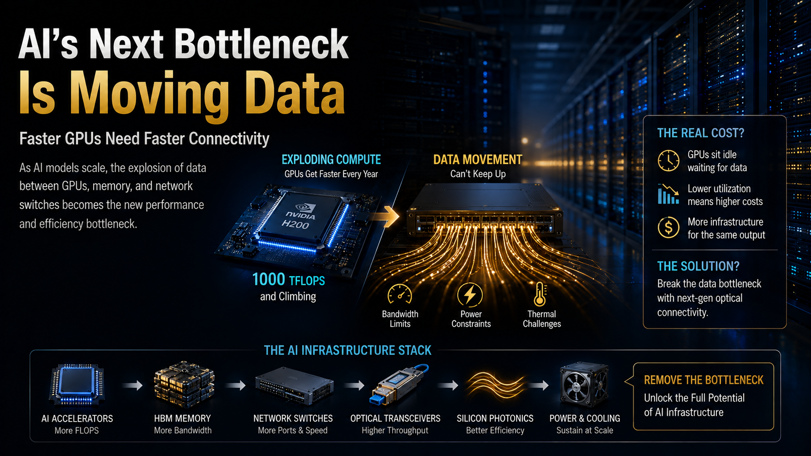
A GPU can perform an extraordinary number of calculations, but its economic value falls if it spends too much time waiting for data from memory, another accelerator, or a network switch.
This is why the AI infrastructure race is gradually expanding beyond raw computing performance.
The next question is no longer simply
How powerful is the chip?
It is also
How efficiently can thousands of powerful chips communicate with one another?
That question is bringing silicon photonics into the center of the AI infrastructure conversation.
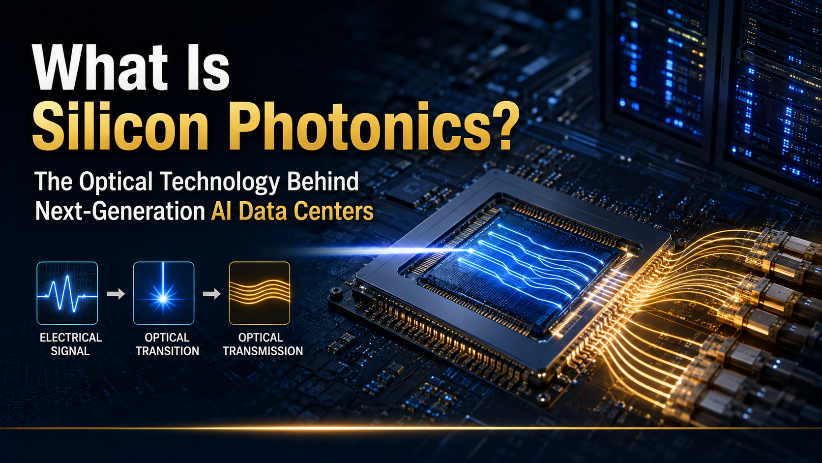
Silicon photonics combines semiconductor manufacturing techniques with optical communication, allowing information to be transmitted using photons rather than relying exclusively on electrical signals.
For investors, the significance extends beyond another semiconductor technology.
Silicon photonics could become part of a broader transition in which the AI investment cycle moves from compute to memory, networking, optical connectivity, advanced packaging, and power efficiency.
The Bottom Line
Silicon photonics uses semiconductor technology to transmit data with light and could help address the bandwidth, power, and thermal challenges created by increasingly large AI computing clusters.
Its importance is not simply that light can move information quickly.
The bigger issue is whether optical connectivity can be integrated economically into semiconductor and data-center architectures at massive scale.
What Is Silicon Photonics?
Silicon photonics is a technology that uses silicon-based semiconductor manufacturing techniques to create integrated optical components for transmitting and processing information.
Traditional computing systems rely heavily on electrical signals.
Data moves between CPUs, GPUs, memory, switches, and other components through electrical interconnects.
This architecture has worked remarkably well for decades.
But the challenge becomes more difficult as bandwidth requirements rise.
At increasingly high data rates, electrical interconnects can face greater problems related to
- power consumption,
- signal integrity,
- heat,
- transmission distance,
- and bandwidth scalability.
Silicon photonics introduces another option.
Instead of transmitting all high-speed information electrically, some data can be converted from electrical signals into optical signals, transmitted using light, and then converted back into electrical form at the destination.
A simple way to think about it is this
Traditional electrical interconnects are highways carrying increasingly heavy traffic.
Silicon photonics creates an optical express lane for the parts of the system where electrical transmission becomes increasingly expensive or inefficient.
This distinction matters.
Silicon photonics does not mean copper connections will suddenly disappear.
Electrical interconnects remain highly effective across many short distances.
The economic opportunity emerges where the cost of moving data electrically begins to rise faster than the benefits of staying with conventional architecture.
How Does Silicon Photonics Work?
The basic process can be simplified into five stages
Electrical signal → Optical conversion → Optical transmission → Optical detection → Electrical signal
Several components make this possible.
Laser Source
Optical communication requires a source of light.
One important technical challenge is that silicon itself is not an ideal material for efficiently generating laser light.
As a result, silicon photonics systems can use external lasers or integrate other semiconductor materials better suited to producing light.
This is why the silicon photonics ecosystem extends beyond silicon itself and can involve compound semiconductors, laser suppliers, packaging companies, and specialized manufacturing technologies.
Modulator
A modulator takes electrical information generated by a processor or networking chip and encodes that information onto an optical signal.
In simple terms, it allows electronic data to travel using light.
Optical Waveguide
The waveguide acts as a pathway for light.
Just as metal traces route electrical signals through conventional electronics, optical waveguides guide photons through an integrated photonic circuit.
Photodetector
At the receiving end, a photodetector detects the optical signal and enables the information to be converted back into an electrical form that processors and other electronic components can use.
The real innovation, therefore, is not simply the use of light.
It is the ability to integrate optical functions into manufacturing processes and packages that increasingly resemble the economics and scale of the semiconductor industry.

Why Use Silicon?
Fiber-optic communication has existed for decades.
Long-distance telecommunications networks already transmit enormous amounts of information using light.
So why is silicon photonics considered such an important development?
The answer is integration and manufacturing economics.
Traditional optical systems can require multiple discrete components that must be manufactured, aligned, packaged, and assembled.
That complexity can increase cost.
Silicon photonics attempts to integrate more optical functionality into compact photonic integrated circuits while leveraging manufacturing techniques developed by the semiconductor industry.
The long-term goal is therefore not simply
Make optical communication faster.
It is
Bring the performance advantages of optics into a scalable semiconductor manufacturing ecosystem.
That difference is fundamental to the investment thesis.
Why Electrical Interconnects Are Becoming a Bigger Challenge
Copper has been extraordinarily successful.
It is inexpensive, familiar, and efficient across many short-distance connections.
Silicon photonics should therefore not be viewed as a universal replacement for electrical connectivity.
The challenge appears as bandwidth and distance increase.
Higher-speed electrical signaling can require increasingly sophisticated circuitry to maintain signal integrity.
That can mean additional power consumption.
And in AI infrastructure, power has become one of the industry's most important constraints.
Consider a cluster containing thousands of AI accelerators.
Those processors are not operating independently.
They constantly exchange model parameters, activations, gradients, and other data.
As the amount of communication rises, the energy required to move information becomes increasingly important.
This changes the economic question facing data-center operators.
It is no longer enough to ask
How much power does the GPU consume?
They must also ask
How much energy does the entire system consume moving data between GPUs?
This is where optical connectivity becomes strategically important.
Why Silicon Photonics Matters for AI Data Centers
Traditional data centers were largely built around servers.
AI infrastructure is increasingly built around clusters.
Training and serving advanced AI models can require large numbers of accelerators operating together as if they were components of one enormous computing machine.
That changes the definition of performance.
A high-performance GPU sitting idle while waiting for data is expensive unused capacity.
The performance of an AI system therefore depends on several layers working together
Compute → Memory → Connectivity
The first phase of the AI infrastructure boom was dominated by compute.
Demand for AI accelerators surged.
As accelerators became more powerful, memory bandwidth became increasingly important, helping push HBM into the center of the semiconductor investment story.
But adding more accelerators creates another problem.
They must communicate.
As AI clusters scale from hundreds to thousands and potentially much larger configurations, networking performance becomes increasingly important.
The AI race is evolving from a competition to build the fastest individual processors into a competition to connect enormous numbers of processors as efficiently as possible.
That is the structural reason silicon photonics matters.
The AI Bottleneck Keeps Moving
One useful way for investors to understand the AI infrastructure cycle is to follow the bottleneck.
A simplified progression looks like this
Compute → Memory → Networking → Power and Cooling
These constraints do not appear one at a time or completely disappear when another becomes important.
They coexist.
But as one bottleneck is reduced, another can become more economically significant.
This also helps explain how capital spending can spread through the AI supply chain.
More AI accelerators require more HBM.
More accelerators and memory require faster networking.
Faster networking increases demand for optical transceivers and other connectivity technologies.
As optical connectivity moves closer to the processor, silicon photonics and advanced packaging become increasingly relevant.
And every additional layer requires power and cooling infrastructure.
This leads to one of the most important lessons for investors studying AI
The AI infrastructure boom is not a single semiconductor cycle. It is a chain of bottlenecks, and capital tends to move toward whichever bottleneck becomes most expensive to ignore.
Silicon Photonics vs. CPO: What Is the Difference?
Silicon photonics is often discussed alongside Co-Packaged Optics, or CPO.
They are closely related, but they are not the same thing.
| Category | Silicon Photonics | Co-Packaged Optics |
| What it is | Integrated optical technology based on semiconductor manufacturing | An architecture that places optical engines close to major chips |
| Primary purpose | Generate, modulate, route, and detect optical signals | Reduce the distance traveled by very high-speed electrical signals |
| Main domain | Photonic integrated circuits | Packaging, switches, and system architecture |
| Potential benefit | Bandwidth density and energy efficiency | Lower I/O power and reduced signal-loss challenges |
| Relationship | Can provide core technology used in CPO | One important application architecture for silicon photonics |
The simplest distinction is
Silicon photonics is the technology. CPO is one way that optical technology can be integrated into a computing or networking system.
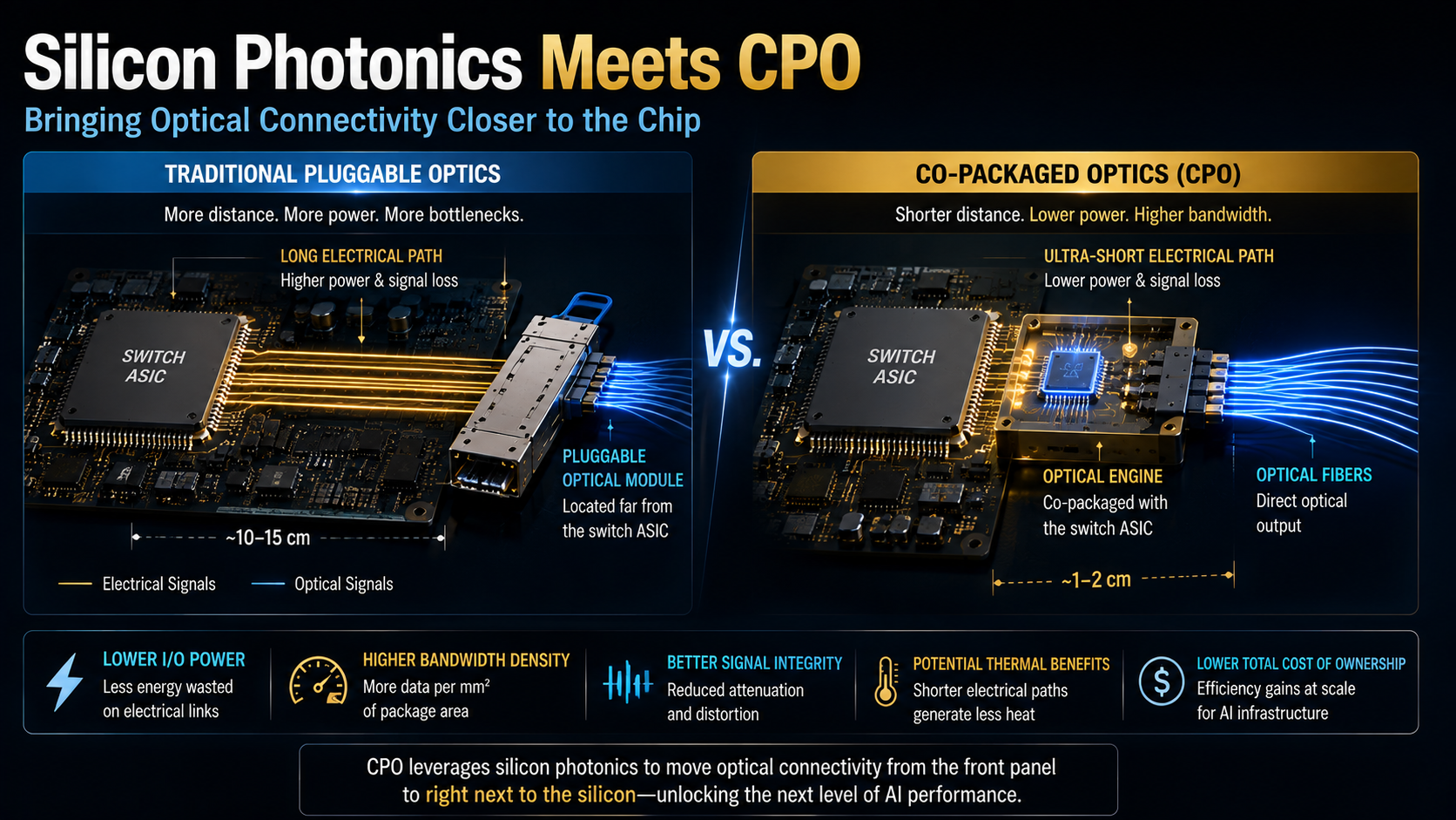
In conventional pluggable optical architectures, electrical signals must travel between a switch ASIC and optical modules located at the front of the system.
As data rates increase, that electrical path becomes more challenging.
CPO moves optical engines closer to the switch silicon, shortening the high-speed electrical connection before the signal becomes optical.
The potential advantages include lower I/O power, greater bandwidth density, and improved signal integrity.
But investors should avoid assuming CPO will immediately replace every pluggable optical module.
Pluggable optics continue to improve as well.
Cost, reliability, serviceability, thermal management, and industry standards will determine how quickly different architectures are adopted.
The transition is more likely to be evolutionary than instantaneous.
Silicon Photonics and the Power Problem
Electricity is becoming one of the defining constraints of the AI data-center buildout.
For hyperscalers, the question is increasingly not only how many GPUs can be purchased but how much computing capacity can actually be deployed within available power and cooling limits.
That makes efficiency economically valuable.
For optical connectivity, one of the metrics that could become increasingly important is not simply maximum bandwidth.
It is energy per bit.
If the amount of data moving through an AI cluster increases dramatically while energy consumption per bit remains too high, networking itself can become a major power burden.
Moving optical conversion closer to high-bandwidth chips could help reduce the energy required across certain high-speed electrical links.
This means the next generation of networking competition may increasingly be defined by
How much data can be moved per unit of power?
For AI infrastructure investors, that is a more important question than headline transmission speed alone.
Why Silicon Photonics Matters to U.S. Investors
For investors, silicon photonics should not be viewed as an isolated technology theme.
It belongs within the broader AI infrastructure capital-expenditure cycle.
The value chain can be simplified as
AI Accelerators → HBM → Network Switches → Optical Transceivers → Silicon Photonics → Advanced Packaging → Power and Cooling
This does not mean capital simply moves from one industry to the next and abandons the previous one.
Instead, the addressable infrastructure stack expands.
When hyperscalers deploy more accelerators, they also need more memory, networking, optical connectivity, power distribution, and cooling.
That means the economic impact of AI spending can spread far beyond the companies designing the processors.
For investors, the better question is therefore not
What is the next AI stock?
It is
Where is the next infrastructure bottleneck, and which part of the supply chain captures the economics of solving it?
How Silicon Photonics Could Affect the AI Infrastructure Value Chain
The most direct investment implications are likely to appear within semiconductors, networking, and data-center infrastructure rather than across every financial asset.
| Industry | Potential Impact |
| Semiconductor Foundries | Additional demand for photonic integrated circuit manufacturing |
| Advanced Packaging | Greater importance of integrating electronic and optical components |
| Optical Networking | Growing demand for high-speed transceivers, optical engines, and lasers |
| Network Equipment | Increasing optical content as AI cluster bandwidth rises |
| Hyperscalers | Potential improvements in network efficiency and total cost of ownership |
| Power & Cooling | Efficiency gains may coexist with continued growth in total AI power demand |
| Broader Macro Assets | Direct impact is limited compared with interest rates, inflation, or monetary policy |
There is an important nuance here.
Improving efficiency does not necessarily reduce total electricity demand.
If better networking makes AI computing cheaper and easier to scale, companies may simply deploy more computing capacity.
In economics, efficiency improvements can sometimes increase total consumption because the underlying activity becomes more attractive.
AI infrastructure could follow a similar pattern.
The amount of energy required to move each bit may decline while the total number of bits being moved rises much faster.
The Challenges Facing Silicon Photonics
A promising technology does not automatically become a profitable industry.
Silicon photonics still faces several important challenges.
Laser Integration
Silicon is not naturally ideal for efficient light generation.
Integrating external lasers or compound semiconductor materials adds complexity to manufacturing and packaging.
Packaging Complexity
Electronic and optical components must be connected with extremely high precision.
Optical coupling and fiber alignment can create manufacturing challenges that do not exist in conventional electronic packaging.
Manufacturing Yield
A prototype demonstrating excellent performance is very different from a product that can be manufactured by the millions at attractive yields.
For investors, yield is critical because poor manufacturing economics can erase the financial benefits of superior technology.
Thermal Management
AI accelerators and networking chips generate significant heat.
Some optical components are sensitive to temperature changes.
Moving optics closer to high-power silicon therefore creates both performance opportunities and thermal engineering challenges.
Reliability and Serviceability
Pluggable optical modules have an obvious operational advantage: they can be replaced relatively easily.
If optical components are integrated deeper into a package, failures can become more complicated and expensive to service.
For this reason, the silicon photonics transition will ultimately be determined by more than bandwidth.
Investors should watch
Cost + Yield + Reliability + Standards + Serviceability + Power Efficiency
What Investors Should Watch
Investors following silicon photonics should avoid treating every company associated with the term as an automatic beneficiary.
Several indicators matter more.
1. AI Network Bandwidth Growth
The fundamental demand driver is the amount of data moving through AI clusters.
If cluster sizes and network bandwidth requirements continue rising, the economic incentive for advanced optical connectivity strengthens.
2. How Close Optics Move to Compute
Historically, optical communication has primarily connected systems across longer distances.
A major structural change would be optics moving progressively closer to servers, switches, packages, and potentially compute itself.
The closer optical connectivity moves toward the processor, the larger the potential role for integrated photonics.
3. CPO Adoption
Product announcements are not the same as commercial adoption.
Investors should watch real deployments, customer qualification, manufacturing scale, and design wins.
4. Manufacturing Economics
Performance alone does not create a mass market.
The winning architecture must eventually deliver acceptable performance at an economically attractive cost.
Yield, packaging complexity, and manufacturing scale therefore matter enormously.
5. Supply-Chain Position
Silicon photonics is not a single-component industry.
The ecosystem includes lasers, photonic integrated circuits, foundries, packaging, testing, transceivers, switches, and system vendors.
The most valuable position in the chain may not necessarily belong to the company receiving the most publicity.
6. Revenue and Free Cash Flow
Emerging technologies often generate excitement long before they generate profits.
Ultimately, investors need evidence that technological leadership is turning into customer adoption, revenue growth, margins, and free cash flow.
Financial markets can price technological potential early, but long-term enterprise value is ultimately validated by cash flow.

What Would Long-Term Capital Look For?
Sophisticated investors do not need to predict exactly which optical architecture will dominate ten years from now.
They need to understand how the economics of the system are changing.
Follow the Capital
The first phase of the generative AI boom concentrated enormous attention on GPUs.
The investment opportunity has since broadened into HBM, networking, optical connectivity, advanced packaging, power generation, electrical infrastructure, and cooling.
The lesson is simple
Capital follows bottlenecks.
When one constraint becomes expensive enough, investment flows toward technologies capable of removing it.
Follow the Cash Flow
A technologically impressive company is not necessarily a financially attractive business.
Long-term investors should distinguish between companies participating in demonstrations and companies winning high-volume production programs.
Watch customer adoption, revenue, gross margins, capital intensity, and free cash flow.
Focus on Survivability
Technology transitions rarely unfold exactly as expected.
Pluggable optics may remain competitive longer than anticipated.
CPO adoption could accelerate or take longer than expected.
Alternative architectures could emerge.
That uncertainty makes financial resilience important.
The question is not only whether a company can win if one technology roadmap succeeds.
It is whether the company can survive if the transition takes longer or develops differently.
Think in Decades, Not Product Cycles
The most important long-term question is
Will the cost and energy required to move data become a structural constraint as AI computing continues to scale?
If the answer is yes, the next question becomes
Which companies capture the economic value created by removing that constraint?
And investors should ultimately ask themselves
Am I investing in excitement around a new technology, or in a structural transition that is beginning to generate durable cash flow?
Prediction matters less than survival.
The companies that endure major technology transitions are often those with the balance sheets, intellectual property, customer relationships, manufacturing capabilities, and cash flows needed to adapt when the original forecast turns out to be wrong.
The Future of Silicon Photonics
The history of computing is partly a history of moving bottlenecks.
Faster processors increased the importance of memory.
Powerful AI accelerators increased the importance of HBM.
Large accelerator clusters are now increasing the importance of networking.
And massive data centers are increasing the importance of power and cooling.
The next generation of AI infrastructure therefore cannot be understood through transistor scaling alone.
Increasingly, system performance depends on the combination of
Compute + Memory + Connectivity + Packaging + Power
Silicon photonics sits primarily within the connectivity layer, but its impact reaches into packaging, networking, semiconductor manufacturing, and data-center economics.
If optical communication continues moving from connections between data centers toward connections inside racks, servers, and packages, the traditional boundary between the semiconductor industry and the optical networking industry could become increasingly blurred.
That is the bigger structural story.
The long-term value of silicon photonics will not be determined by whether it produces another bandwidth record.
It will be determined by whether it can reduce the economic cost of moving enormous amounts of data through increasingly large AI computing systems.
Final Thoughts
Silicon photonics combines semiconductor manufacturing with optical communication to move information using light.
Its growing relevance to AI comes from a simple problem
Computing power is scaling faster than our ability to move data efficiently between computing resources.
As AI infrastructure expands, the bottleneck is no longer confined to the GPU.
It moves through the entire system
Compute → Memory → Networking → Optical Connectivity → Packaging → Power
Silicon photonics could become an important part of solving the connectivity portion of that equation.
But investors should avoid the simplistic conclusion that silicon photonics is "the next big technology" and therefore every company associated with it will benefit.
Technology adoption depends on economics.
Cost, manufacturing yield, reliability, standards, customer adoption, packaging complexity, and competition from improving electrical and pluggable optical technologies will all matter.
The more durable investment insight is broader
Watch where the AI infrastructure bottleneck moves next—and then follow where capital, competitive advantage, and ultimately cash flow move with it.
The AI era will not be defined only by how quickly machines can compute.
It will increasingly be defined by how efficiently enormous computing systems can move data.
Silicon photonics is one of the technologies attempting to solve that challenge.
This was MasterMind.
'[Global] Success Blueprints' 카테고리의 다른 글