What Is a Chiplet? How Chiplet Technology Is Reshaping AI Chips and the Semiconductor Industry


Hello, this is MasterMind.
Why are companies like NVIDIA, AMD, Intel, TSMC, and even Apple moving away from building one massive chip and instead designing processors made up of multiple smaller chips?
For decades, the semiconductor industry advanced by shrinking transistors and packing more of them into a single piece of silicon. But as manufacturing approaches physical and economic limits, the rules of chip design are changing.
Today, the next competitive advantage isn't simply building smaller chips—it's building smarter systems.
That is where Chiplet technology comes in.
In this article, we'll explore what Chiplets are, how they work, why they have become essential in the AI era, and what this structural shift means for long-term investors.
Key Takeaway
A Chiplet is a modular semiconductor architecture that combines multiple specialized chips into a single package, delivering higher performance, better manufacturing yields, lower costs, and greater scalability than traditional monolithic chip designs.
What Is a Chiplet?
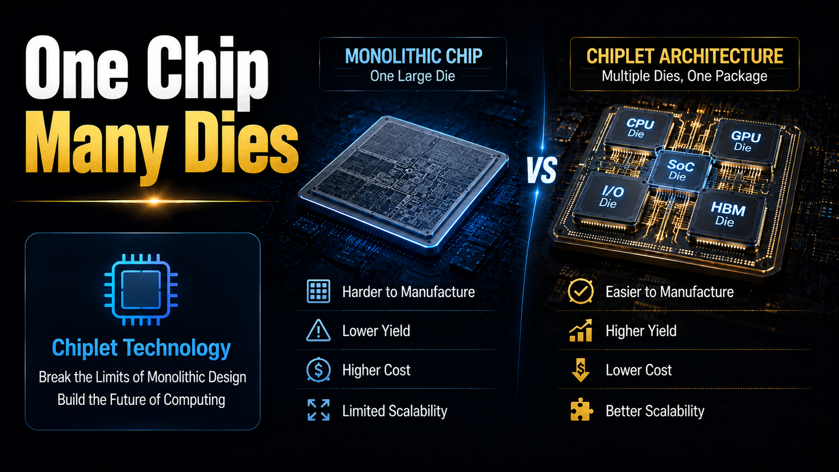
For years, most processors were built using a monolithic design, meaning every function—including CPU cores, GPU cores, cache, memory controllers, and I/O—was manufactured on one large silicon die.
This approach worked well when transistor scaling consistently reduced costs and improved performance.
However, modern semiconductor manufacturing has reached a point where making a single massive chip is becoming increasingly expensive and technically difficult.
Instead of creating one enormous processor, Chiplet architecture divides a processor into multiple smaller dies, each optimized for a specific task.
These smaller dies are then connected through advanced packaging technologies so they function as one unified processor.
Think of it like constructing a skyscraper.
Instead of pouring one giant concrete structure at once, engineers build highly specialized modules independently before assembling them into a complete building. The result is faster construction, lower risk, and greater flexibility.
The same principle applies to modern semiconductor manufacturing.
How Does Chiplet Technology Work?
Chiplets solve several of the biggest challenges facing today's semiconductor industry.
1. Better Manufacturing Yield
Large chips are difficult to manufacture.
Even a microscopic defect on a wafer can render an entire processor unusable.
As chip size increases, the probability of defects rises significantly, reducing manufacturing yield and increasing production costs.
Smaller chiplets dramatically improve yield because defective dies can simply be discarded individually rather than throwing away an entire large processor.
For manufacturers, this translates into:
- Higher production efficiency
- Lower manufacturing costs
- Better profitability
2. Heterogeneous Integration
Not every component inside a processor requires the most advanced manufacturing node.
For example:
- CPU cores may benefit from 2nm or 3nm manufacturing.
- I/O controllers often perform perfectly well on mature 6nm or even 12nm processes.
- Analog circuitry may require completely different process technologies.
Chiplets allow each component to be manufactured using the process technology that offers the best balance between performance and cost.
This approach significantly improves overall economics without sacrificing computing power.
3. Advanced Packaging Makes Everything Work Together
Separating chips creates a new challenge:
How can multiple dies communicate as efficiently as one?
The answer lies in advanced packaging.
Technologies such as:
- TSMC CoWoS
- Intel Foveros
- Intel EMIB
- AMD Infinity Fabric
- UCIe (Universal Chiplet Interconnect Express)
allow multiple chiplets to exchange data at extremely high bandwidth while minimizing latency and power consumption.
In many cases, software treats the entire package as if it were a single processor.

Why Chiplets Matter
The semiconductor industry's next race is no longer about making one chip smaller. It's about connecting multiple chips more efficiently than anyone else.
This represents one of the biggest architectural shifts since Moore's Law became the industry's guiding principle.
Moore's Law Is Facing Economic Limits
Transistors continue to shrink, but each new manufacturing node costs dramatically more than the previous generation.
Extreme Ultraviolet (EUV) lithography, higher mask counts, and increasingly complex fabrication processes have made cutting-edge semiconductor manufacturing extraordinarily expensive.
Chiplets provide a practical way to continue improving performance without placing every function on the latest—and most expensive—process node.
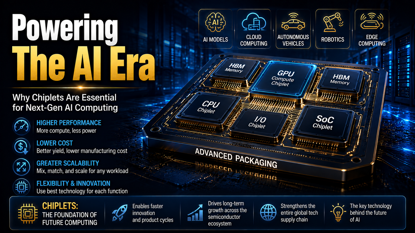
AI Computing Is Driving Demand
Artificial intelligence is transforming semiconductor design.
Training and deploying large language models requires enormous computing resources, including:
- Massive GPU clusters
- High-bandwidth memory (HBM)
- AI accelerators
- Ultra-fast interconnects
Modern AI processors increasingly rely on Chiplet architectures because scaling a single monolithic die has become impractical.
This is one reason advanced packaging has become one of the hottest investment themes across the semiconductor industry.
How Chiplets Are Reshaping the Semiconductor Industry
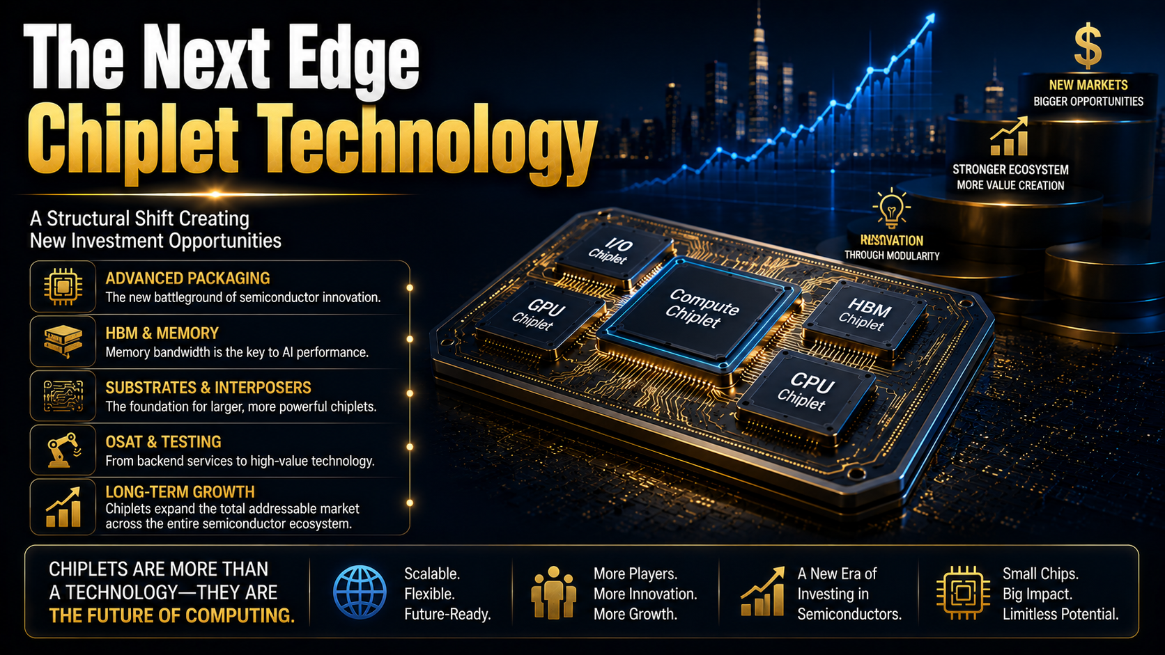
| Sector | Long-Term Impact |
| Foundries | Greater demand for advanced packaging capabilities alongside leading-edge process nodes. |
| Advanced Packaging | Strategic importance continues to rise as AI processors become increasingly complex. |
| OSAT Companies | Packaging and testing evolve from low-margin services into high-value technologies. |
| HBM Manufacturers | Memory bandwidth becomes a key differentiator for AI performance. |
| Substrate Suppliers | FC-BGA and future glass substrates gain importance for larger multi-die packages. |
| EDA & IP Companies | Chiplet design software and interconnect IP become increasingly valuable. |
The industry's center of gravity is gradually expanding beyond wafer fabrication.
Future semiconductor leadership will depend not only on transistor technology but also on packaging, interconnects, software, substrates, and system-level integration.
Key Investment Takeaways
Advanced Packaging Is Becoming a Competitive Advantage
The AI era has elevated packaging from a manufacturing step into a strategic capability.
Companies capable of integrating multiple chiplets efficiently may gain significant competitive advantages.
UCIe Could Become the Industry Standard
Just as USB standardized peripheral connectivity, UCIe aims to standardize communication between chiplets built by different companies.
If widely adopted, it could accelerate ecosystem growth while lowering development costs across the industry.
Semiconductor Supply Chains Are Becoming More Valuable
AI hardware requires far more than powerful processors.
Growth increasingly benefits:
- Packaging companies
- Memory manufacturers
- High-end substrate suppliers
- Semiconductor IP developers
- Design automation software providers
Understanding where value is shifting may become more important than simply identifying the fastest processor.
What Are Professional Investors Watching?
Professional investors rarely focus only on the newest chip.
Instead, they analyze where capital is flowing throughout the semiconductor ecosystem.
During previous technology cycles, most investment attention centered on process-node leadership.
Today, capital is expanding toward advanced packaging, HBM memory, substrate technologies, chip interconnects, and AI infrastructure.
This reflects a broader structural transition.
The semiconductor industry is evolving from competition between individual chips to competition between complete ecosystems.
Massive AI infrastructure spending also illustrates this trend.
Billions of dollars invested in hyperscale data centers do not benefit GPU manufacturers alone. Those investments ripple across memory suppliers, packaging specialists, substrate producers, networking companies, and semiconductor equipment manufacturers.
Markets consistently reward businesses that solve the industry's biggest bottlenecks.
In the AI era, one of those bottlenecks is no longer transistor density—it's how efficiently data moves between chips.
Rather than attempting to predict every technological winner, long-term investors may benefit more from understanding how capital allocation evolves as semiconductor architectures change.
Consider asking yourself:
- Which companies are building the infrastructure that enables AI rather than simply selling AI chips?
- Where is the semiconductor industry's value creation moving over the next decade?
- Which businesses benefit regardless of which GPU manufacturer ultimately wins market share?
- Am I investing in products, or in the broader ecosystem supporting them?
Final Thoughts
Chiplets are far more than a new chip design technique.
They represent a fundamental shift in how the semiconductor industry will continue delivering performance improvements despite the physical and economic limits of transistor scaling.
As AI, cloud computing, autonomous vehicles, robotics, and edge computing continue to grow, Chiplet architectures are likely to become the foundation of next-generation computing platforms.
For investors, the most important takeaway is that semiconductor leadership is no longer defined solely by who builds the smallest transistor.
Increasingly, it will be defined by who can integrate, package, and connect the world's most advanced chips into the most efficient computing systems.
Understanding that shift may prove far more valuable than simply following quarterly earnings reports.
This was MasterMind.
'[Global] Success Blueprints' 카테고리의 다른 글