What Is an Interposer? How It Connects AI Chips and HBM and Why It Matters


Hello, this is MasterMind.
When investors think about the AI semiconductor boom, the conversation usually starts with GPUs, high-bandwidth memory (HBM), and advanced process nodes.
But there is another part of the AI hardware stack that receives far less attention.
How can a powerful AI accelerator communicate with multiple stacks of HBM fast enough to keep its computing engines fully utilized?
Building a faster GPU is only part of the solution. The data feeding that GPU must also move at enormous speed and with high energy efficiency.
This is where the interposer becomes important.
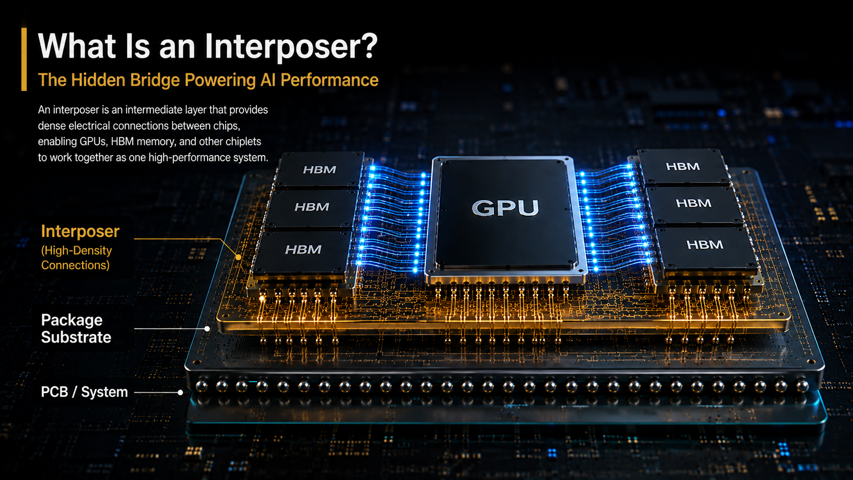
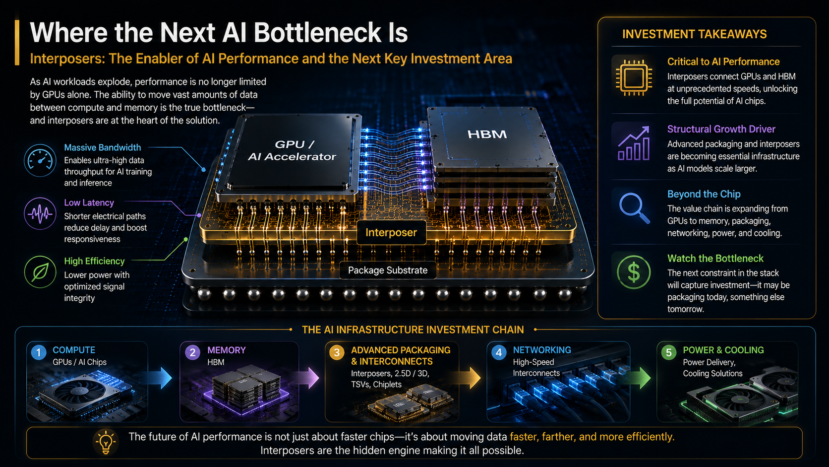
An interposer is not simply a platform that holds semiconductor dies together. It is a high-density connectivity layer that helps GPUs, AI accelerators, HBM, and other chiplets communicate as part of a single high-performance package.
As AI computing becomes increasingly constrained by memory bandwidth, packaging capacity, power consumption, and data movement, understanding interposers can help investors see a much broader shift taking place across the semiconductor industry.
Key Takeaway
An interposer is an intermediate connectivity layer that uses dense electrical connections to integrate GPUs, AI accelerators, HBM, and other semiconductor dies into a high-performance package. In the AI era, it has become an important part of solving the data-movement bottleneck between computing and memory.
What Is an Interposer?
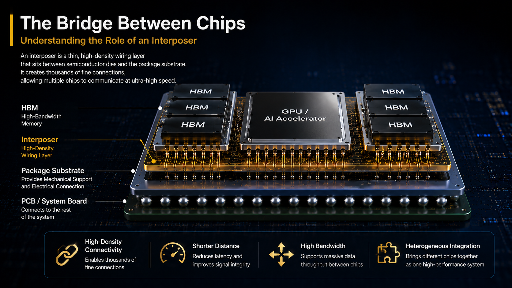
An interposer is an intermediate layer positioned between semiconductor dies and the underlying package substrate.
Its primary purpose is to provide dense electrical connections between multiple chips.
A simplified AI accelerator package might look like this
[ HBM ]     [ GPU / AI Accelerator ]     [ HBM ]
    \                  |                    /
     └─────────── Interposer ─────────────┘
                       |
                Package Substrate
                       |
                     System
The interposer can contain extremely fine wiring that allows large numbers of signals to travel between the processor and memory.
One way to understand the concept is to think about transportation infrastructure.
Imagine the GPU as a massive industrial city and HBM as a group of enormous logistics centers.
It does not matter how productive the city is or how much inventory the warehouses contain if the highways connecting them cannot handle the traffic.
The interposer effectively provides those high-capacity highways.
This becomes increasingly important as AI accelerators require enormous amounts of data to move between compute engines and memory.
Why Did the Semiconductor Industry Need Interposers?
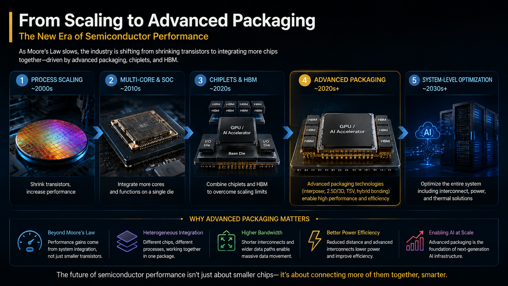
For decades, semiconductor performance improvements were largely associated with putting more transistors onto increasingly advanced process nodes.
That model remains important, but it has become more expensive and technically challenging.
There is also another problem.
Not every function inside a modern computing system necessarily needs to be manufactured using the same leading-edge process.
This has encouraged the semiconductor industry to increasingly combine multiple dies within a single package.
These dies can include
- CPU cores
- GPU or AI accelerator dies
- I/O dies
- HBM
- Specialized chiplets
Instead of treating packaging as simply the final step after a semiconductor has been manufactured, advanced packaging increasingly becomes part of the system architecture itself.
The interposer is one technology that helps make this possible.
How Does an Interposer Work?
The importance of interposers can be understood through three fundamental functions.
1. It Shortens the Distance Between Chips
Distance matters in semiconductor systems.
Longer electrical connections can make it more difficult to maintain signal integrity while increasing latency and energy consumption.
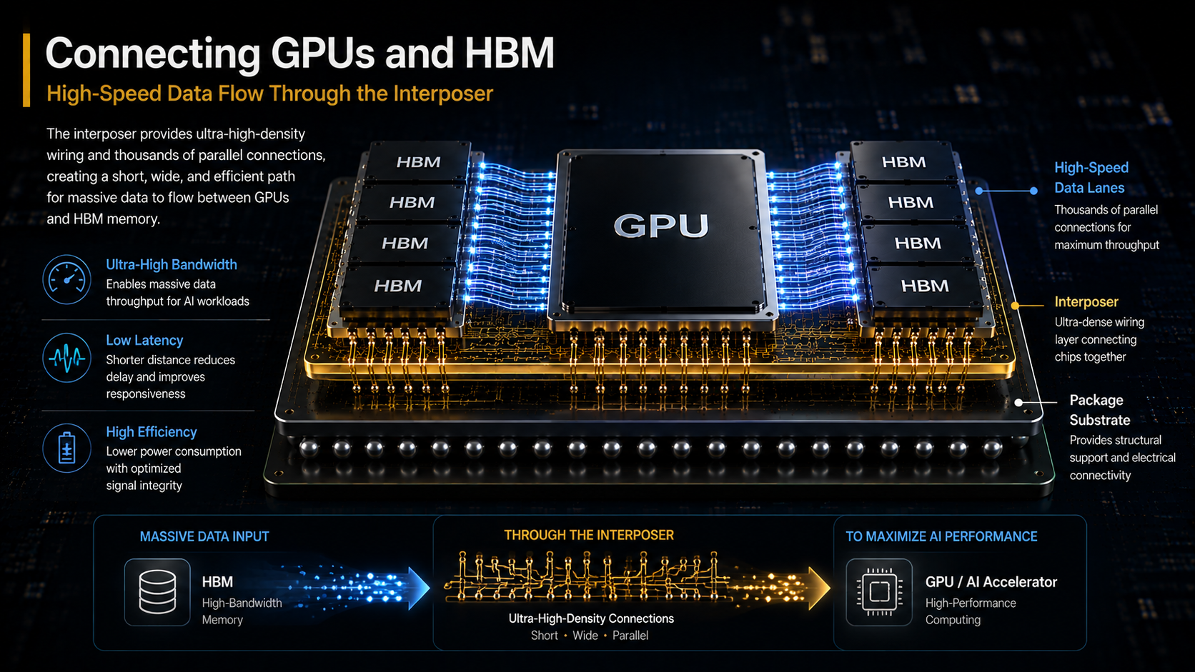
An interposer allows components such as GPUs and HBM to sit extremely close together within the same package.
The basic relationship is straightforward
Shorter connections → more efficient signaling → higher bandwidth → better system performance
This is especially important for AI workloads, where massive amounts of data must continuously move between memory and compute resources.
2. It Creates More Data Pathways
A powerful AI accelerator is only useful when it can receive data quickly enough to perform its calculations.
HBM addresses this challenge by providing an extremely wide memory interface and high bandwidth.
But that bandwidth also requires a large number of physical connections between memory and the processor.
Dense interposer wiring helps provide these parallel data pathways.
Instead of relying on a relatively small number of connections traveling longer distances across a conventional board, advanced packaging can create thousands of much shorter connections inside the package.
3. It Integrates Multiple Chips Into One System
Modern high-performance processors increasingly consist of multiple components rather than one giant monolithic die.
Interposers can help connect GPUs, CPUs, I/O dies, HBM, and other chiplets so they behave more like one integrated computing system.
This architecture is closely associated with 2.5D packaging, which has become particularly important in high-performance computing and AI accelerators.
Interposers vs. TSV: What Is the Difference?
Investors researching advanced packaging will frequently encounter another acronym: TSV, or Through-Silicon Via.
The two concepts are related, but they are not the same thing.
A TSV is a vertical electrical connection that passes through silicon.
In some silicon-interposer architectures, TSVs can provide vertical connections between components above the interposer and the package substrate below.
The interposer, by contrast, is the broader intermediate connectivity structure.
In simple terms
Interposer = connectivity platform
TSV = one method of creating vertical electrical connections
This distinction matters because advanced packaging is evolving rapidly.
Not every future architecture will necessarily rely on exactly the same combination of silicon interposers and TSVs.
Bridge technologies, organic materials, glass-based solutions, hybrid bonding, and other packaging approaches are expanding the industry's options.
Silicon, Organic, and Glass Interposers
The term "interposer" does not describe one single material.
Different materials and architectures offer different trade-offs involving wiring density, cost, package size, manufacturing complexity, and yield.
| Technology | Characteristics | Potential Advantages | Key Challenges |
| Silicon Interposer | Silicon-based fine wiring | Very high interconnect density | Cost, size and manufacturing complexity |
| Organic Interposer | Organic substrate materials | Potentially lower cost and larger area | Fine-line wiring limitations |
| Glass Interposer | Glass-based structure | Potential dimensional stability and large-format scalability | Manufacturing maturity and yield |
| Silicon Bridge | Silicon used only where dense connections are required | Reduces the amount of silicon needed | Design and manufacturing complexity |
One important investment lesson follows from this comparison.
A new material does not automatically make the previous technology obsolete.
Different AI accelerators require different combinations of bandwidth, package size, thermal performance, manufacturing cost, and yield.
The semiconductor industry may therefore support multiple packaging architectures simultaneously.
For long-term investors, the more useful question is not simply
"Which material will win?"
A better question is
Which architecture offers the best balance of performance, cost, manufacturability, and yield for a particular workload?
Why Are Interposers Important for AI?
AI Is Increasingly a Data-Movement Problem
The AI semiconductor race is often described as a competition for more computing power.
That is only part of the story.
Large AI models require enormous amounts of data to move continuously between memory and processing units.
A GPU can theoretically perform tremendous numbers of calculations per second, but those computing resources cannot be fully utilized if the processor spends too much time waiting for data.
This is one reason memory bandwidth has become such an important part of AI hardware design.
HBM increases the amount of data that can reach an AI processor.
Advanced packaging and interconnect technologies help make that bandwidth usable at the system level.
This leads to a broader insight about the AI infrastructure cycle
The AI semiconductor race is increasingly about eliminating bottlenecks across compute, memory, interconnects, networking, power, and cooling—not simply building a faster chip.
Interposers sit directly inside that transition.
Moore's Law and the Rise of Advanced Packaging
The increasing importance of interposers does not mean transistor scaling has suddenly become irrelevant.
Leading-edge manufacturing remains critical.
But the economics of semiconductor development are changing.
As process nodes become more advanced, semiconductor design and manufacturing become increasingly expensive and complex.
This creates an incentive to improve system performance in additional ways.
A simplified industry progression looks like this
Advanced Process Scaling
          ↓
Higher Design and Manufacturing Costs
          ↓
Greater Use of Chiplets and HBM
          ↓
Multiple Dies Integrated Into One Package
          ↓
Need for Dense Interconnects
          ↓
Growing Importance of Advanced Packaging
The key change is that semiconductor performance is increasingly being optimized at several levels simultaneously.
Transistor technology still matters.
But so do memory architecture, packaging, chip-to-chip communication, networking, software, power efficiency, and cooling.
For investors, this expands the semiconductor value chain far beyond the leading-edge wafer fab.
Interposers and Advanced Packaging
Interposers should be understood as part of the much larger advanced packaging ecosystem.
Traditional semiconductor packaging was often viewed primarily as a way to protect a finished chip and connect it to a circuit board.
AI computing has changed that perception.
Packaging architecture can now directly influence bandwidth, latency, energy efficiency, package size, and overall system performance.
That is why technologies such as the following have become strategically important
- 2.5D packaging
- 3D stacking
- Chiplets
- Silicon interposers
- Silicon bridges
- Hybrid bonding
- High-density substrates
The boundary between semiconductor manufacturing and semiconductor packaging is becoming less distinct.
Increasingly, both must be optimized together.
What Does CoWoS Have to Do With Interposers?
One term U.S. semiconductor investors frequently encounter alongside AI accelerators and HBM is CoWoS, or Chip-on-Wafer-on-Substrate.
CoWoS is a major advanced packaging architecture used to integrate high-performance processors and memory within the same package.
The rapid growth of AI accelerator demand demonstrated something important about semiconductor economics
The number of AI chips that can be sold is not determined solely by how many processor dies can be manufactured.
HBM availability matters.
Advanced packaging capacity matters.
Substrate availability matters.
Testing and assembly capacity matter.
The entire supply chain must move together.
If one critical step cannot expand quickly enough, that step can become the constraint on final system shipments.
This is why investors increasingly monitor packaging capacity alongside GPU and HBM production.
How Interposers Affect the Semiconductor Market
Interposers do not influence financial markets in the same direct way that interest rates or inflation do.
Their significance comes from the structural expansion of AI infrastructure spending.
| Industry | Potential Impact |
| Foundry & Advanced Packaging | Greater strategic value for high-density packaging capacity |
| HBM | Growth increasingly tied to packaging and AI accelerator integration |
| Semiconductor Equipment | Potential demand for bonding, TSV, deposition, inspection and metrology equipment |
| Materials & Substrates | Greater requirements for high-performance packaging materials |
| AI Chip Designers | Packaging and memory availability can influence shipment volumes |
| Hyperscalers | AI server deployment can be affected by semiconductor supply-chain constraints |
This creates an important framework for analyzing the AI investment cycle.
Capital often begins by concentrating on the most visible beneficiary.
In AI, that has frequently been the accelerator itself.
But as infrastructure spending expands, investors begin looking for the next constraint.
Conceptually, the chain can be viewed as
GPU → HBM → Advanced Packaging & Interconnects → Networking → Power & Cooling
This should not be interpreted as a fixed chronological sequence.
Instead, it illustrates how capital can migrate toward whichever part of the infrastructure stack becomes the next bottleneck.
What Does This Mean for U.S. Investors?
The interposer theme is primarily relevant to equities rather than macro assets such as Treasury bonds, gold, or the U.S. dollar.
For semiconductor investors, however, it can reveal where value is being created across the AI supply chain.
Semiconductor Stocks
Higher AI accelerator demand can increase the strategic importance of advanced packaging, HBM integration, substrates, bonding, inspection, metrology, and related semiconductor equipment.
But investors should distinguish between industry growth and shareholder returns.
A rapidly growing market does not guarantee that every company exposed to that market will generate attractive returns.
Competition, capital intensity, customer concentration, pricing power, and technological substitution still matter.
Bonds
The direct relationship is limited.
However, the extraordinary capital expenditures associated with AI infrastructure can affect corporate financing requirements, cash flows, debt issuance, and balance-sheet strategies across the technology ecosystem.
U.S. Dollar
There is little direct relationship between interposer technology and the dollar.
The broader connection comes through the role of U.S.-based technology companies in global AI investment and international capital flows.
Gold
Interposers have virtually no direct relationship with gold prices.
Real interest rates, monetary policy, the dollar, inflation expectations, central-bank demand, and geopolitical risk are substantially more important drivers.
Bitcoin
There is also little direct causal relationship between interposers and Bitcoin.
Both AI-related equities and crypto assets can sometimes benefit from broader risk appetite and liquidity conditions, but that should not be confused with a fundamental technology connection.
What Should Investors Watch?
1. Look Beyond HBM
HBM demand is important, but memory must ultimately be integrated into an AI accelerator package.
Investors should therefore examine the entire chain connecting memory to compute.
A shortage in packaging capacity can matter even when sufficient processor and memory dies exist.
2. Watch Yield, Not Just Capacity
Semiconductor manufacturing is not simply about theoretical production capacity.
A technology must be manufactured economically and reliably at scale.
As AI packages become larger and more complicated, yield can become increasingly important.
Announcements about new capacity should therefore be evaluated alongside production yield, customer qualification, manufacturing stability, and utilization.
3. Monitor the Evolution of Interposer Materials
Silicon remains important, but the industry continues to develop organic, bridge-based, glass, and other approaches.
Investors should avoid assuming that one technology will dominate every application.
Instead, monitor four variables
Performance, cost, yield, and scalability.
4. Follow the Entire Packaging Value Chain
As advanced packaging becomes strategically important, value can spread across
- Materials
- Packaging equipment
- Bonding
- Inspection
- Metrology
- Substrates
- Design IP
- Testing
The most attractive economics may not always sit with the most visible company.
5. Separate Technology Growth From Business Quality
A rapidly growing technology can still produce disappointing investment returns if too much capital enters the market.
The key questions are whether a company has pricing power, durable customer relationships, differentiated technology, and barriers that prevent competitors from quickly expanding capacity.
What Do Long-Term Capital Allocators Look For?
Long-term investors usually ask a different question from traders chasing the latest semiconductor theme.
Instead of asking
"Which stocks are related to interposers?"
They ask
Where is the next structural bottleneck in AI infrastructure, and which businesses can turn that bottleneck into durable cash flow?
Follow the Money
During the early stages of an AI investment cycle, capital may concentrate around GPUs and software.
As infrastructure spending expands, investment can spread toward HBM, advanced packaging, interconnects, networking, power equipment, and cooling.
Markets often reward not only the companies creating demand, but also the businesses solving the constraints that prevent that demand from being fulfilled.
Follow the Cash Flow
A good technology is not automatically a good investment.
Technological advantages must eventually translate into revenue, margins, and free cash flow.
If packaging capacity expands faster than demand, shortages can disappear and pricing power can weaken.
Investors should therefore monitor both sides of the equation
Demand growth and supply growth.
Look for Survivability
AI is developing quickly enough that today's critical technology may not occupy exactly the same position several years from now.
That makes adaptability important.
Companies with diversified customers, strong balance sheets, manufacturing expertise, intellectual property, and the ability to participate in multiple packaging architectures may be better positioned to survive technological transitions.
Think in Decades, Not Product Cycles
Investing is not about perfectly predicting which packaging architecture will dominate every future AI accelerator.
It is about finding businesses that can survive when the future develops differently from expectations.
Investors can ask
- Which components become more important as AI processors become more powerful?
- Where is capacity currently constrained?
- Is that bottleneck temporary or structural?
- Does the company have genuine pricing power?
- Is technological leadership translating into free cash flow?
- How quickly can competitors add capacity?
- Can the company adapt if packaging architecture changes?
- How much future growth is already reflected in the valuation?
Those questions help separate long-term semiconductor analysis from simply chasing an AI theme.
Final Thoughts
An interposer is an intermediate connectivity layer that helps integrate GPUs, AI accelerators, HBM, and other semiconductor dies into a high-performance package.
Its importance reflects a broader transformation in the semiconductor industry.
For decades, one of the industry's defining questions was
How much smaller can we make the transistor?
That question remains important.
But AI has added another
How efficiently can we connect increasingly powerful chips together?
As GPU performance increases, memory bandwidth becomes more important. As HBM becomes faster, packaging and interconnect technology must evolve alongside it.
That means investors analyzing AI semiconductors should look beyond individual processors and examine the entire infrastructure stack
Compute → Memory → Advanced Packaging & Interconnects → Networking → Power & Cooling
The long-term lesson is straightforward.
Capital flows toward growth, but some of the most important opportunities can emerge where companies remove the bottlenecks preventing that growth from continuing.
That is why interposers deserve attention.
The AI semiconductor race is no longer only about how quickly an individual chip can calculate. It is increasingly about how efficiently compute, memory, and connectivity can function together as one system.
This was MasterMind.
'[Global] Success Blueprints' 카테고리의 다른 글